Serial audio interface (SAI) RM0351
1328/1693 DocID024597 Rev 3
Refer to Section 39.3.9: AC’97 link controller for details on clock generator programming in
AC’97 mode and to Section 39.3.10: SPDIF output for details on clock generator
programming in SPDIF mode.
39.3.7 SAI clock generator
Each audio block has its own clock generator that makes these two blocks completely
independent. There is no difference in terms of functionality between these two clock
generators.
When the audio block is configured as Master, the clock generator provides the
communication clock (the bit clock) and the master clock for external decoders.
When the audio block is defined as slave, the clock generator is OFF.
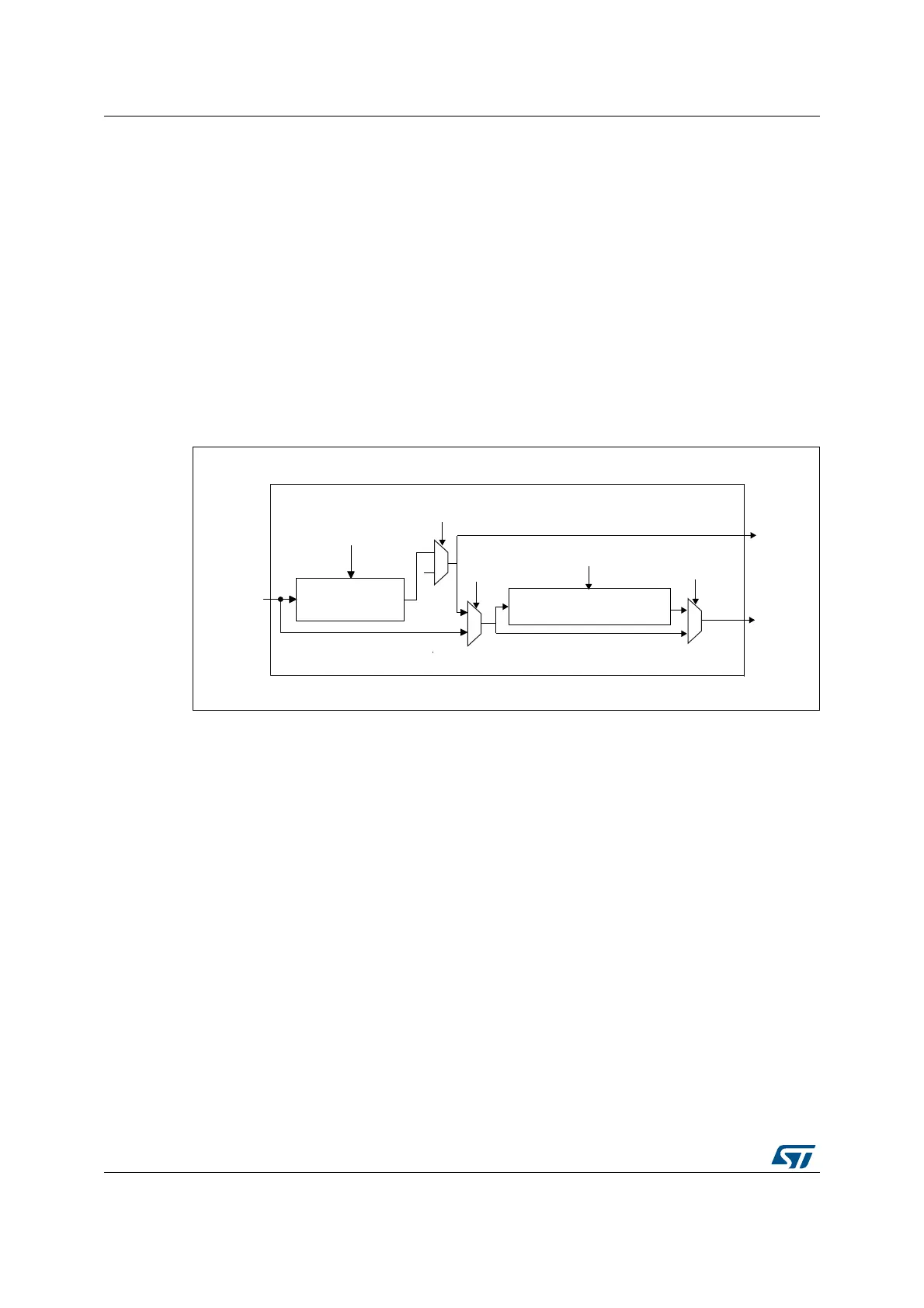
Figure 442 illustrates the architecture of the audio block clock generator.
Figure 442. Audio block clock generator overview
Note: If NODIV is set to 1, the MCLK_x signal will be set at 0 level if this pin is configured as the
SAI pin in GPIO peripherals.
The clock source for the clock generator comes from the product clock controller. The
SAI_CK_x clock is equivalent to the master clock which can be divided for the external
decoders using bit MCKDIV[3:0]:
MCLK_x = SAI_CK_x / (MCKDIV[3:0] * 2), if MCKDIV[3:0] is not equal to 0000.
MCLK_x = SAI_CK_x, if MCKDIV[3:0] is equal to 0000.
MCLK_x signal is used only in TDM.
The division must be even in order to keep 50% on the Duty cycle on the MCLK output and
on the SCK_x clock. If bit MCKDIV[3:0] = 0000, division by one is applied to obtain MCLK_x
equal to SAI_CK_x.
In the SAI, the single ratio MCLK/FS = 256 is considered. Mostly, three frequency ranges
will be encountered as illustrated in Table 209.
06Y9
0&.',9>@
6&.B[
0&/.B[
12',9
12',9
12',9
6$,B&.B[
)5/>@
%LWFORFNGLYLGHU
0DVWHUFORFN
GLYLGHU

 Loading...


