Flexible static memory controller (FSMC) RM0351
386/1693 DocID024597 Rev 3
14.6.1 External memory interface signals
The following tables list the signals that are typically used to interface NAND Flash memory.
Note: The prefix “N” identifies the signals which are active low.
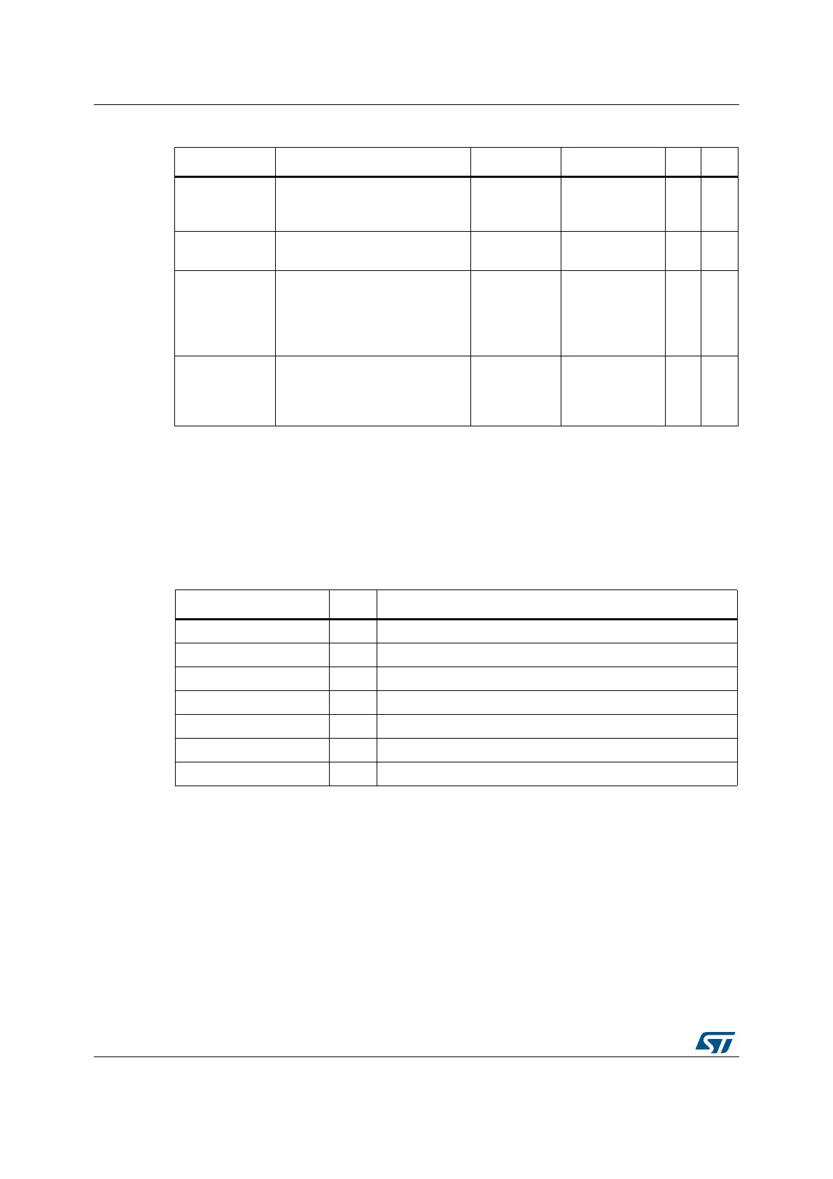
8-bit NAND Flash memory
t
Theoretically, there is no capacity limitation as the FMC can manage as many address
cycles as needed.
Table 76. Programmable NAND Flash access parameters
Parameter Function Access mode Unit Min. Max.
Memory setup
time
Number of clock cycles (HCLK)
required to set up the address
before the command assertion
Read/Write
AHB clock cycle
(HCLK)
1 255
Memory wait
Minimum duration (in HCLK clock
cycles) of the command assertion
Read/Write
AHB clock cycle
(HCLK)
2 255
Memory hold
Number of clock cycles (HCLK)
during which the address must be
held (as well as the data if a write
access is performed) after the
command de-assertion
Read/Write
AHB clock cycle
(HCLK)
1 254
Memory
databus high-Z
Number of clock cycles (HCLK)
during which the data bus is kept
in high-Z state after a write
access has started
Write
AHB clock cycle
(HCLK)
1 255
Table 77. 8-bit NAND Flash
FMC signal name I/O Function
A[17] O NAND Flash address latch enable (ALE) signal
A[16] O NAND Flash command latch enable (CLE) signal
D[7:0] I/O 8-bit multiplexed, bidirectional address/data bus
NCE O Chip Select
NOE(= NRE) O Output enable (memory signal name: read enable, NRE)
NWE O Write enable
NWAIT/INT I NAND Flash ready/busy input signal to the FMC

 Loading...


