DocID024597 Rev 3 537/1693
RM0351 Analog-to-digital converters (ADC)
540
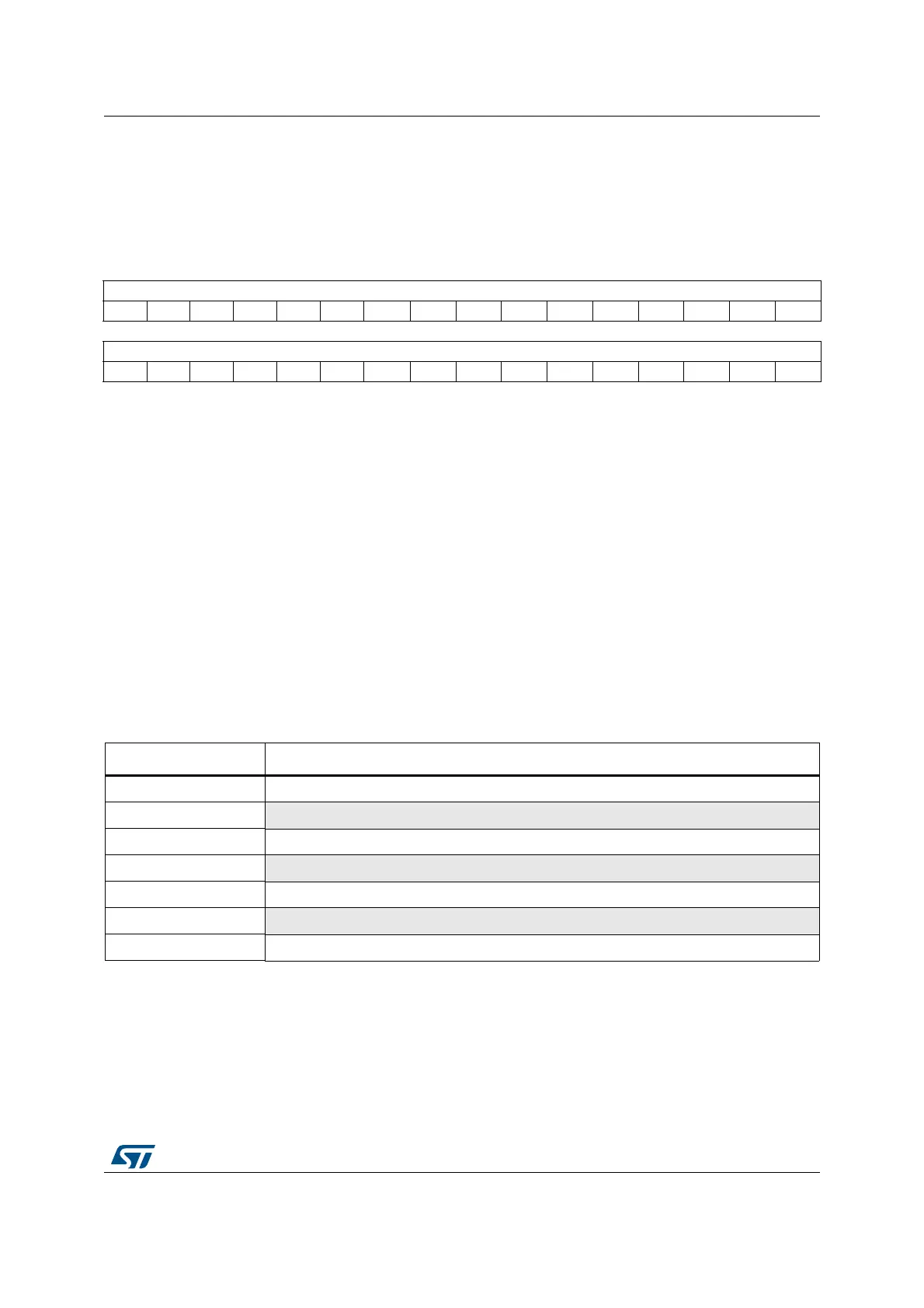
16.6.3 ADC common regular data register for dual mode (ADCx_CDR)
Address offset: 0x0C (this offset address is relative to the master ADC base address +
0x300)
Reset value: 0x0000 0000
16.6.4 ADC register map
The following table summarizes the ADC registers.
31 30 29 28 27 26 25 24 23 22 21 20 19 18 17 16
RDATA_SLV[15:0]
rrrrrr r r r r rrrrrr
1514131211109876543210
RDATA_MST[15:0]
rrrrrr r r r r rrrrrr
Bits 31:16 RDATA_SLV[15:0]: Regular data of the slave ADC
In dual mode, these bits contain the regular data of the slave ADC. Refer to Section 16.3.30:
Dual ADC modes.
The data alignment is applied as described in Section : Data register, data alignment and
offset (ADCx_DR, OFFSETy, OFFSETy_CH, ALIGN))
Bits 15:0 RDATA_MST[15:0]: Regular data of the master ADC.
In dual mode, these bits contain the regular data of the master ADC. Refer to
Section 16.3.30: Dual ADC modes.
The data alignment is applied as described in Section : Data register, data alignment and
offset (ADCx_DR, OFFSETy, OFFSETy_CH, ALIGN))
In MDMA=0b11 mode, bits 15:8 contains SLV_ADC_DR[7:0], bits 7:0 contains
MST_ADC_DR[7:0].
Table 99. ADC global register map
Offset Register
0x000 - 0x0B4 Master ADC1
0x0B8 - 0x0FC Reserved
0x100 - 0x1B4 Slave ADC2
0x1B8 - 0x1FC Reserved
0x200 - 0x2B4 Single ADC3
0x2B8 - 0x2FC
Reserved
0x300 - 0x30C Master and slave ADCs common registers

 Loading...


