Power control (PWR) RM0351
168/1693 DocID024597 Rev 3
5.4.7 Power status clear register (PWR_SCR)
Address offset: 0x18
Reset value: 0x0000 0000.
Access: 3 additional APB cycles are needed to write this register vs. a standard APB write.
5.4.8 Power Port A pull-up control register (PWR_PUCRA)
Address offset: 0x20.
Reset value: 0x0000 0000. This register is not reset when exiting Standby modes and with
PWRRST bit in the RCC_APB1RSTR1 register.
Access: Additional APB cycles are needed to access this register vs. a standard APB
access (3 for a write and 2 for a read).
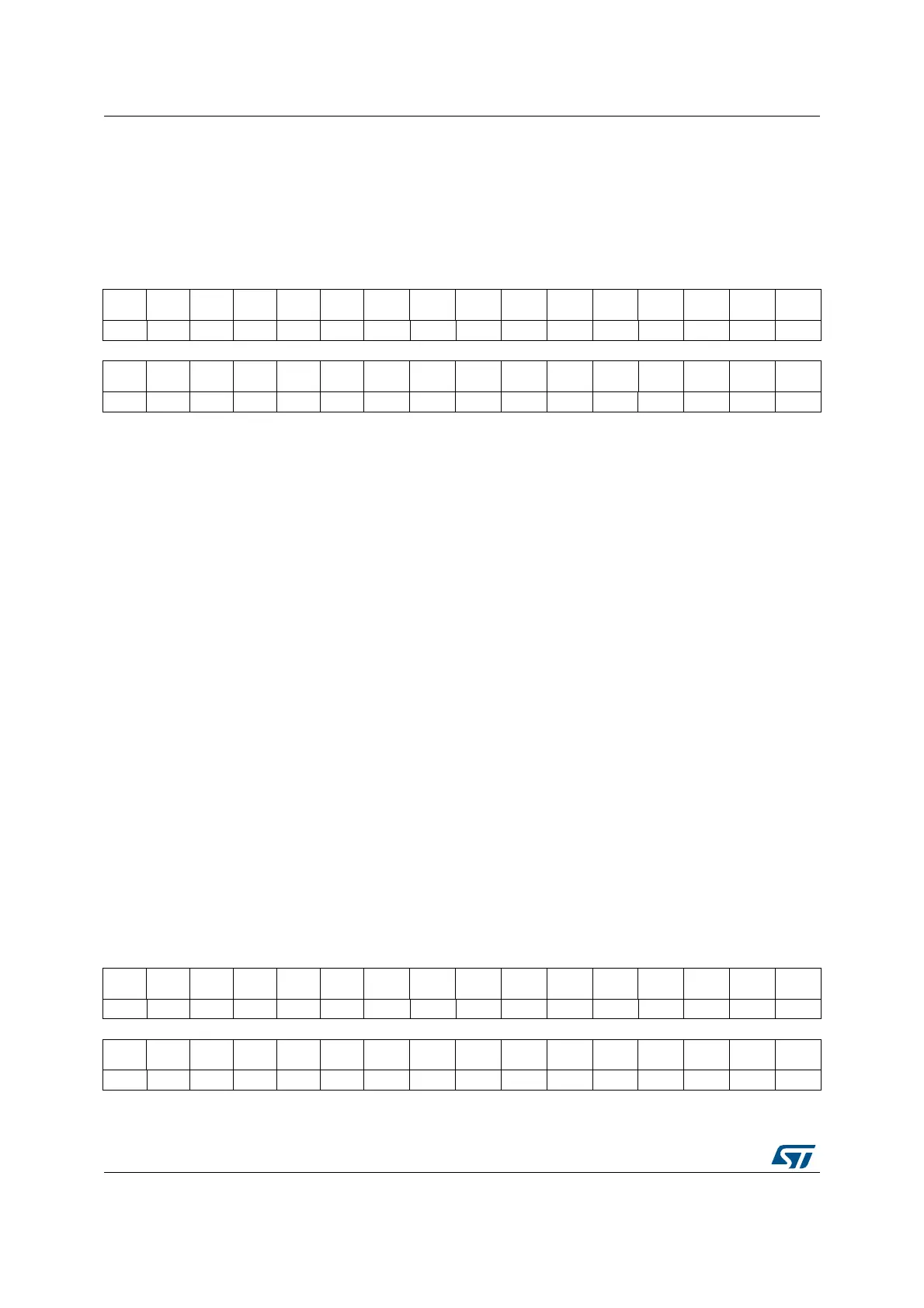
31 30 29 28 27 26 25 24 23 22 21 20 19 18 17 16
Res. Res. Res. Res. Res. Res. Res. Res. Res. Res. Res. Res. Res. Res. Res. Res.
1514131211109876543210
Res. Res. Res. Res. Res. Res. Res. CSBF Res. Res. Res. CWUF5 CWUF4 CWUF3 CWUF2 CWUF1
wwwwww
Bits 31:9 Reserved, must be kept at reset value.
Bit 8 CSBF: Clear standby flag
Setting this bit clears the SBF flag in the PWR_SR1 register.
Bits 7:5 Reserved, must be kept at reset value.
Bit 4 CWUF5: Clear wakeup flag 5
Setting this bit clears the WUF5 flag in the PWR_SR1 register.
Bit 3 CWUF4: Clear wakeup flag 4
Setting this bit clears the WUF4 flag in the PWR_SR1 register.
Bit 2 CWUF3: Clear wakeup flag 3
Setting this bit clears the WUF3 flag in the PWR_SR1 register.
Bit 1 CWUF2: Clear wakeup flag 2
Setting this bit clears the WUF2 flag in the PWR_SR1 register.
Bit 0 CWUF1: Clear wakeup flag 1
Setting this bit clears the WUF1 flag in the PWR_SR1 register.
31 30 29 28 27 26 25 24 23 22 21 20 19 18 17 16
Res. Res. Res. Res. Res. Res. Res. Res. Res. Res. Res. Res. Res. Res. Res. Res.
1514131211109876543210
PU15 Res. PU13 PU12 PU11 PU10 PU9 PU8 PU7 PU6 PU5 PU4 PU3 PU2 PU1 PU0
rw rw rw rw rw rw rw rw rw rw rw rw rw rw rw

 Loading...


