DocID024597 Rev 3 313/1693
RM0351 Direct memory access controller (DMA)
318
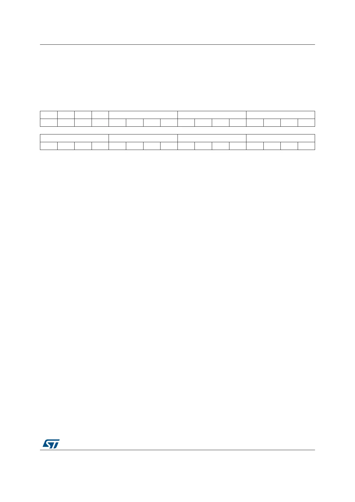
10.5.7 DMA1 channel selection register (DMA1_CSELR)
Address offset: 0xA8 (with respect to DMA1 base address)
Reset value: 0x0000 0000
This register is used to manage the mapping of DMA channels (see Figure 24).
31 30 29 28 27 26 25 24 23 22 21 20 19 18 17 16
Res. Res. Res. Res. C7S [3:0] C6S [3:0] C5S [3:0]
rw rw rw rw rw rw rw rw rw rw rw rw
1514131211109876543210
C4S [3:0] C3S [3:0] C2S [3:0] C1S [3:0]
rw rw rw rw rw rw rw rw rw rw rw rw rw rw rw rw
Bits 31:28 Reserved, must be kept at reset value.
Bits 27:24 C7S[3:0]: DMA channel 7 selection
0000: Channel 7 mapped on DFSDM3
0001: Channel 7 mapped on SAI2_B
0010: Channel 7 mapped on USART2_TX
0011: Channel 7 mapped on I2C1_RX
0100: Channel 7 mapped on TIM2_CH2/TIM2_CH4
0101: Channel 7 mapped on TIM17_CH1/TIM17_UP
0110: Channel 7 mapped on TIM4_UP
0111: Channel 7 mapped on TIM1_CH3
Bits 23:20 C6S[3:0]: DMA channel 6 selection
0000: Channel 6 mapped on DFSDM2
0001: Channel 6 mapped on SAI2_A
0010: Channel 6 mapped on USART2_RX
0011: Channel 6 mapped on I2C1_TX
0100: Channel 6 mapped on TIM16_CH1/TIM16_UP
0101: Channel 6 mapped on TIM3_CH1/TIM3_TRIG
0110: Reserved
0111: Channel 6 mapped on TIM1_UP
others: Reserved
Bits 19:16 C5S[3:0]: DMA channel 5 selection
0000: Channel 5 mapped on DFSDM1
0001: Channel 5 mapped on SPI2_TX
0010: Channel 5 mapped on USART1_RX
0011: Channel 5 mapped on I2C2_RX
0100: Channel 5 mapped on TIM2_CH1
0101: Channel 5 mapped on QUADSPI
0110: Channel 5 mapped on TIM4_CH3
0111: Channel 5 mapped on TIM15_CH1/TIM15_UP/TIM15_TRIG/TIM15_COM
others: Reserved