Reset and clock control (RCC) RM0351
192/1693 DocID024597 Rev 3
6.2.15 Clock-out capability
• MCO
The microcontroller clock output (MCO) capability allows the clock to be output onto the
external MCO pin. One of seven clock signals can be selected as the MCO clock.
–LSI
–LSE
– SYSCLK
–HSI16
–HSE
–PLLCLK
–MSI
The selection is controlled by the MCOSEL[2:0] bits of the Clock configuration register
(RCC_CFGR). The selected clock can be divided with the MCOPRE[2:0] field of the
Clock configuration register (RCC_CFGR).
• LSCO
Another output (LSCO) allows a low speed clock to be output onto the external LSCO
pin:
–LSI
–LSE
This output remains available in Stop (Stop 0, Stop 1 and Stop 2) and Standby modes.
The selection is controlled by the LSCOSEL, and enabled with the LSCOEN in the
Backup domain control register (RCC_BDCR).
The configuration registers of the corresponding GPIO port must be programmed in
alternate function mode.
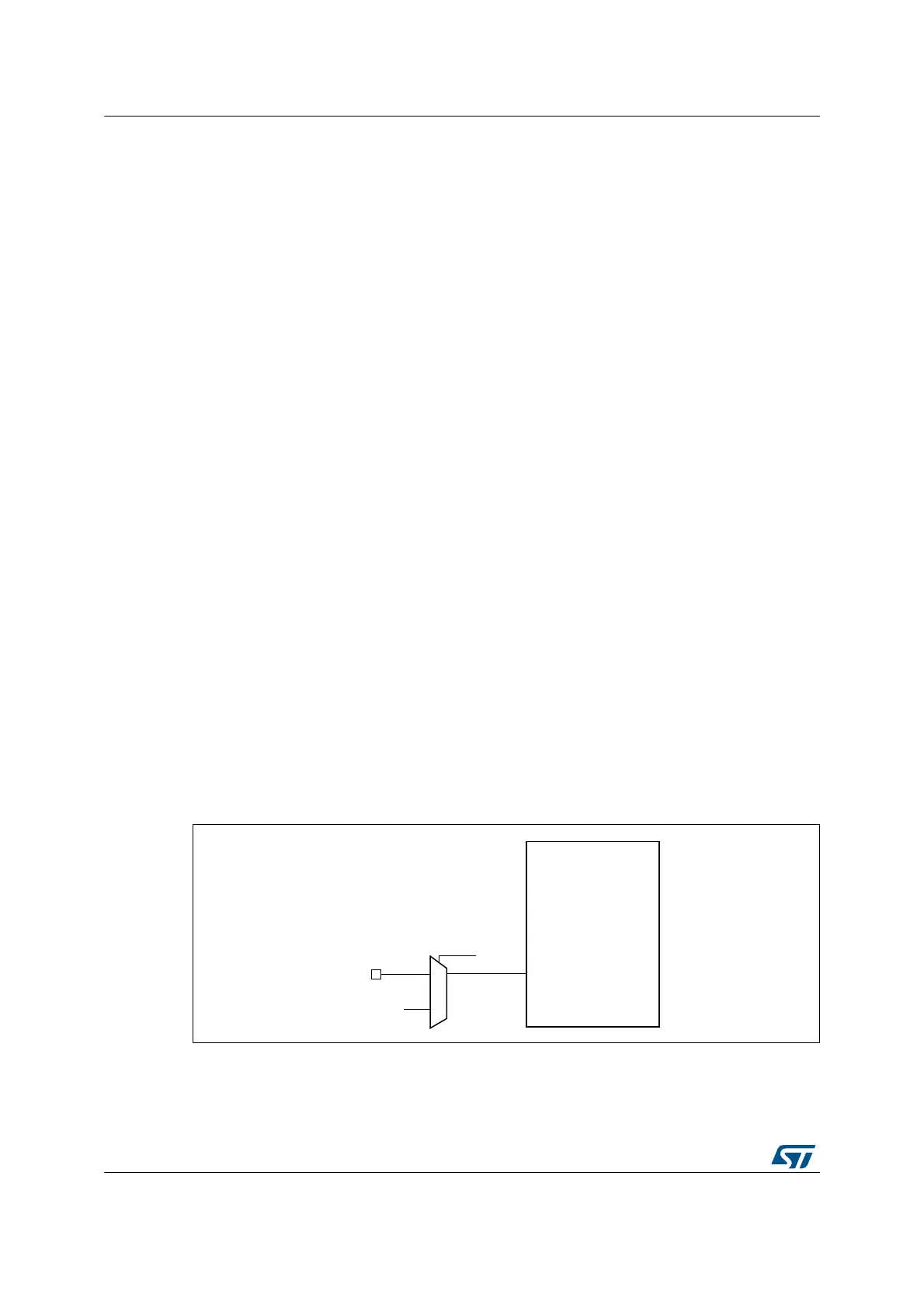
6.2.16 Internal/external clock measurement with TIM15/TIM16/TIM17
It is possible to indirectly measure the frequency of all on-board clock sources by mean of
the TIM15, TIM16 or TIM17 channel 1 input capture, as represented on Figure 14, Figure 15
and Figure 16.
Figure 14. Frequency measurement with TIM15 in capture mode
069
7,0
7,
7,B503
*3,2
/6(

 Loading...


