Reset and clock control (RCC) RM0351
206/1693 DocID024597 Rev 3
6.4.5 PLLSAI1 configuration register (RCC_PLLSAI1CFGR)
Address offset: 0x10
Reset value: 0x0000 1000
Access: no wait state, word, half-word and byte access
This register is used to configure the PLLSAI1 clock outputs according to the formulas:
• f(VCOSAI1 clock) = f(PLL clock input) × (PLLSAI1N / PLLM)
• f(PLLSAI1_P) = f(VCOSAI1 clock) / PLLSAI1P
• f(PLLSAI1_Q) = f(VCOSAI1 clock) / PLLSAI1Q
• f(PLLSAI1_R) = f(VCOSAI1 clock) / PLLSAI1R
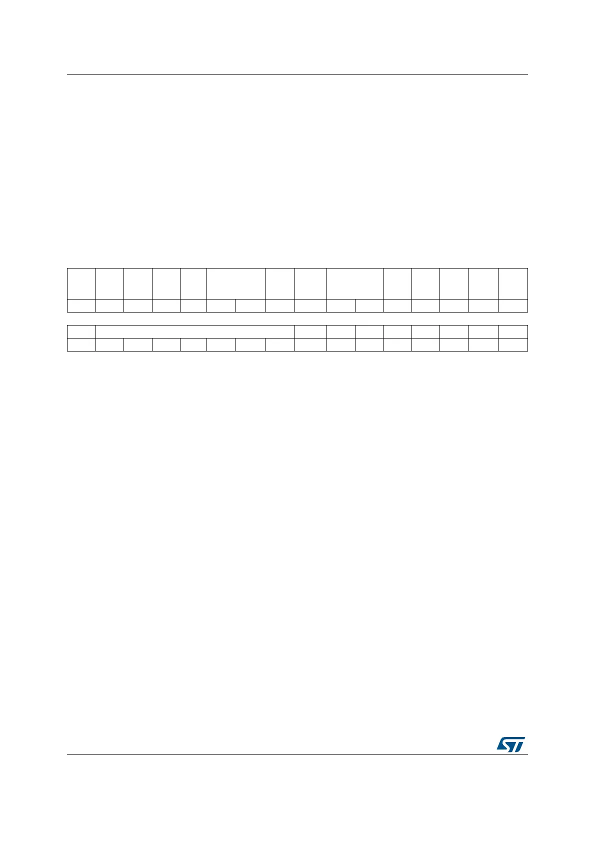
31 30 29 28 27 26 25 24 23 22 21 20 19 18 17 16
Res. Res. Res. Res. Res. PLLSAI1R[1:0]
PLL
SAI1
REN
Res. PLLSAI1Q[1:0]
PLL
SAI1
QEN
Res. Res.
PLL
SAI1P
PLL
SAI1
PEN
rw rw rw rw rw rw rw rw
1514131211109 8 7 654321 0
Res. PLLSAI1N[6:0] Res. Res. Res. Res. Res. Res. Res. Res.
rw rw rw rw rw rw rw
Bits 31:27 Reserved, must be kept at reset value.
Bits 26:25 PLLSAI1R[1:0]: PLLSAI1 division factor for PLLADC1CLK (ADC clock)
Set and cleared by software to control the frequency of the SAI1PLL output clock
PLLADC1CLK. This output can be selected as ADC clock. These bits can be written only if
SAI1PLL is disabled.
PLLADC1CLK output clock frequency = VCOSAI1 frequency / PLLSAI1R with PLLSAI1R =
2, 4, 6, or 8
00: PLLSAI1R = 2
01: PLLSAI1R = 4
10: PLLSAI1R = 6
11: PLLSAI1R = 8
Bit 24 PLLSAI1REN: PLLSAI1 PLLADC1CLK output enable
Set and reset by software to enable the PLLADC1CLK output of the SAI1PLL (used as clock
for ADC).
In order to save power, when the PLLADC1CLK output of the SAI1PLL is not used, the value
of PLLSAI1REN should be 0.
0: PLLADC1CLK output disable
1: PLLADC1CLK output enable
Bit 23 Reserved, must be kept at reset value.

 Loading...


