Flexible static memory controller (FSMC) RM0351
348/1693 DocID024597 Rev 3
14.4.2 NAND Flash memory address mapping
The NAND bank is divided into memory areas as indicated in Table 48.
For NAND Flash memory, the common and attribute memory spaces are subdivided into
three sections (see in Table 49 below) located in the lower 256 Kbytes:
• Data section (first 64 Kbytes in the common/attribute memory space)
• Command section (second 64 Kbytes in the common / attribute memory space)
• Address section (next 128 Kbytes in the common / attribute memory space)
The application software uses the 3 sections to access the NAND Flash memory:
• To sending a command to NAND Flash memory, the software must write the
command value to any memory location in the command section.
• To specify the NAND Flash address that must be read or written, the software
must write the address value to any memory location in the address section. Since an
address can be 4 or 5 bytes long (depending on the actual memory size), several
consecutive write operations to the address section are required to specify the full
address.
• To read or write data, the software reads or writes the data from/to any memory
location in the data section.
Since the NAND Flash memory automatically increments addresses, there is no need to
increment the address of the data section to access consecutive memory locations.
1. In case of a 16-bit external memory width, the FMC will internally use HADDR[25:1] to generate the
address for external memory FMC_A[24:0].
Whatever the external memory width, FMC_A[0] should be connected to external memory address A[0].
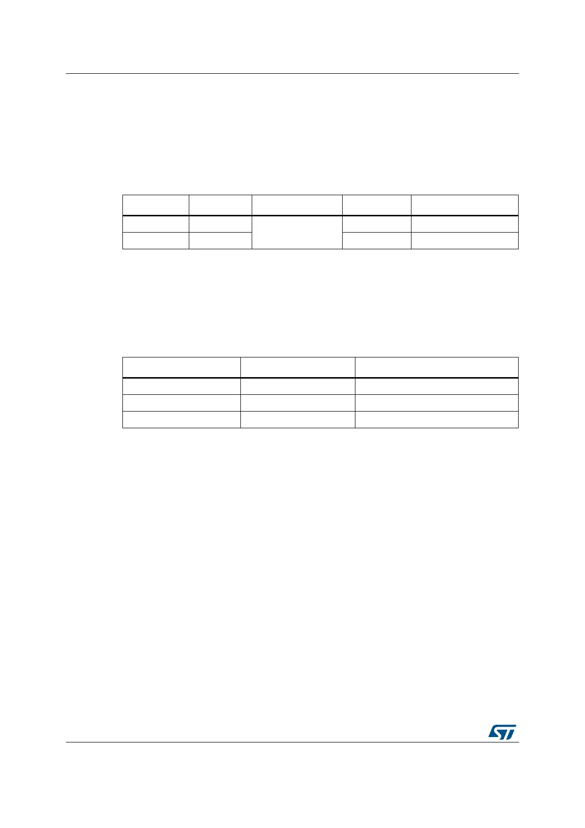
Table 48. NAND memory mapping and timing registers
Start address End address FMC bank Memory space Timing register
0x8800 0000 0x8BFF FFFF
Bank 3 - NAND Flash
Attribute FMC_PATT (0x8C)
0x8000 0000 0x83FF FFFF Common FMC_PMEM (0x88)
Table 49. NAND bank selection
Section name HADDR[17:16] Address range
Address section 1X 0x020000-0x03FFFF
Command section 01 0x010000-0x01FFFF
Data section 00 0x000000-0x0FFFF