Quad-SPI interface (QUADSPI) RM0351
404/1693 DocID024597 Rev 3
In each phase which is configured in quad mode, IO0/IO1/IO2/IO3 are all are at high-
impedance (input) during the data phase for read operations, and outputs in all other cases.
In the dummy phase when DMODE = 11, IO0/IO1/IO2/IO3 are all high-impedance.
IO2 and IO3 are used only in Quad SPI mode. If none of the phases are configured to use
Quad SPI mode, then the pins corresponding to IO2 and IO3 can be used for other functions
even while QUADSPI is active.
SDR mode
By default, the DDRM bit (QUADSPI_CCR[31]) is 0 and the QUADSPI operates in single
data rate (SDR) mode.
In SDR mode, when the QUADSPI is driving the IO0/SO, IO1, IO2, IO3 signals, these
signals transition only with the falling edge of CLK.
When receiving data in SDR mode, the QUADSPI assumes that the Flash memories also
send the data using CLK’s falling edge. By default (when SSHIFT = 0), the signals are
sampled using the following (rising) edge of CLK.
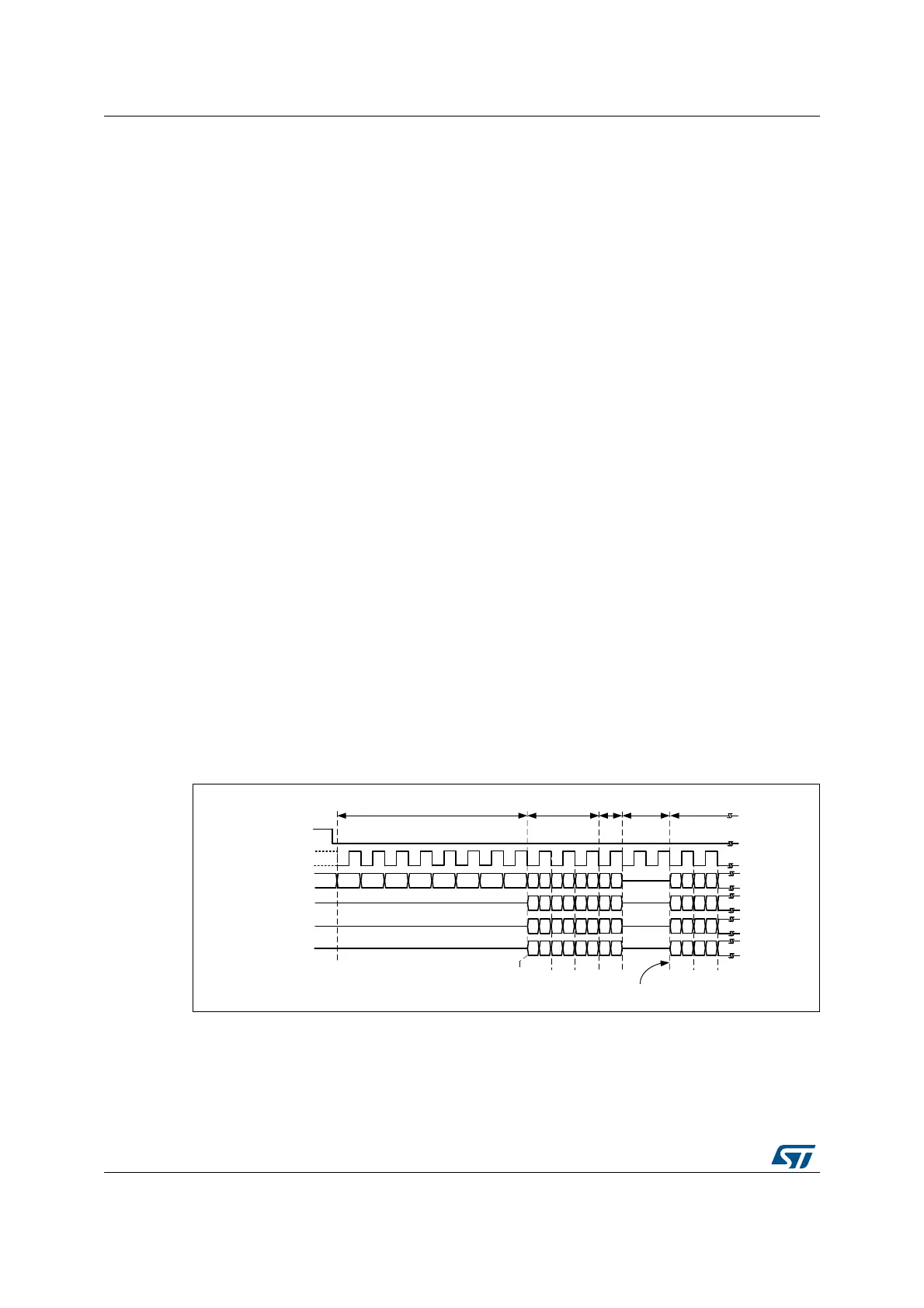
DDR mode
When the DDRM bit (QUADSPI_CCR[31]) is set to 1, the QUADSPI operates in double data
rate (DDR) mode.
In DDR mode, when the QUADSPI is driving the IO0/SO, IO1, IO2, IO3 signals in the
address/alternate-byte/data phases, a bit is sent on each of the falling and rising edges of
CLK.
The instruction phase is not affected by DDRM. The instruction is always sent using CLK’s
falling edge.
When receiving data in DDR mode, the QUADSPI assumes that the Flash memories also
send the data using both rising and falling CLK edges. When DDRM = 1, firmware must
clear SSHIFT bit (QUADSPI_CR[4]). Thus, the signals are sampled one half of a CLK cycle
later (on the following, opposite edge).
Figure 53. An example of a DDR command in quad mode
15.3.4 QUADSPI indirect mode
When in indirect mode, commands are started by writing to QUADSPI registers and data is
transferred by writing or reading the data register, in the same way as for other
communication peripherals.
069
Q&6
6&/.
,2
,2
,2
,2
$
$
0
%\WH
,QVWUXFWLRQ $GGUHVV
$OW 'XPP\ 'DWD
,2VZLWFKIURP
RXWSXWWRLQSXW
$
%\WH