Embedded Flash memory (FLASH) RM0351
92/1693 DocID024597 Rev 3
3.4 FLASH option bytes
3.4.1 Option bytes description
The option bytes are configured by the end user depending on the application requirements.
As a configuration example, the watchdog may be selected in hardware or software mode
(refer to Section 3.4.2: Option bytes programming).
A double word is split up as follows in the option bytes:
The organization of these bytes inside the information block is as shown in Table 10: Option
byte organization.
The option bytes can be read from the memory locations listed in Table 10: Option byte
organization or from the Option byte registers:
• Flash option register (FLASH_OPTR)
• Flash Bank 1 PCROP Start address register (FLASH_PCROP1SR)
• Flash Bank 1 PCROP End address register (FLASH_PCROP1ER)
• Flash Bank 1 WRP area A address register (FLASH_WRP1AR)
• Flash Bank 1 WRP area B address register (FLASH_WRP1BR)
• Flash Bank 2 PCROP Start address register (FLASH_PCROP2SR)
• Flash Bank 2 PCROP End address register (FLASH_PCROP2ER)
• Flash Bank 2 WRP area A address register (FLASH_WRP2AR)
• Flash Bank 2 WRP area B address register (FLASH_WRP2BR).
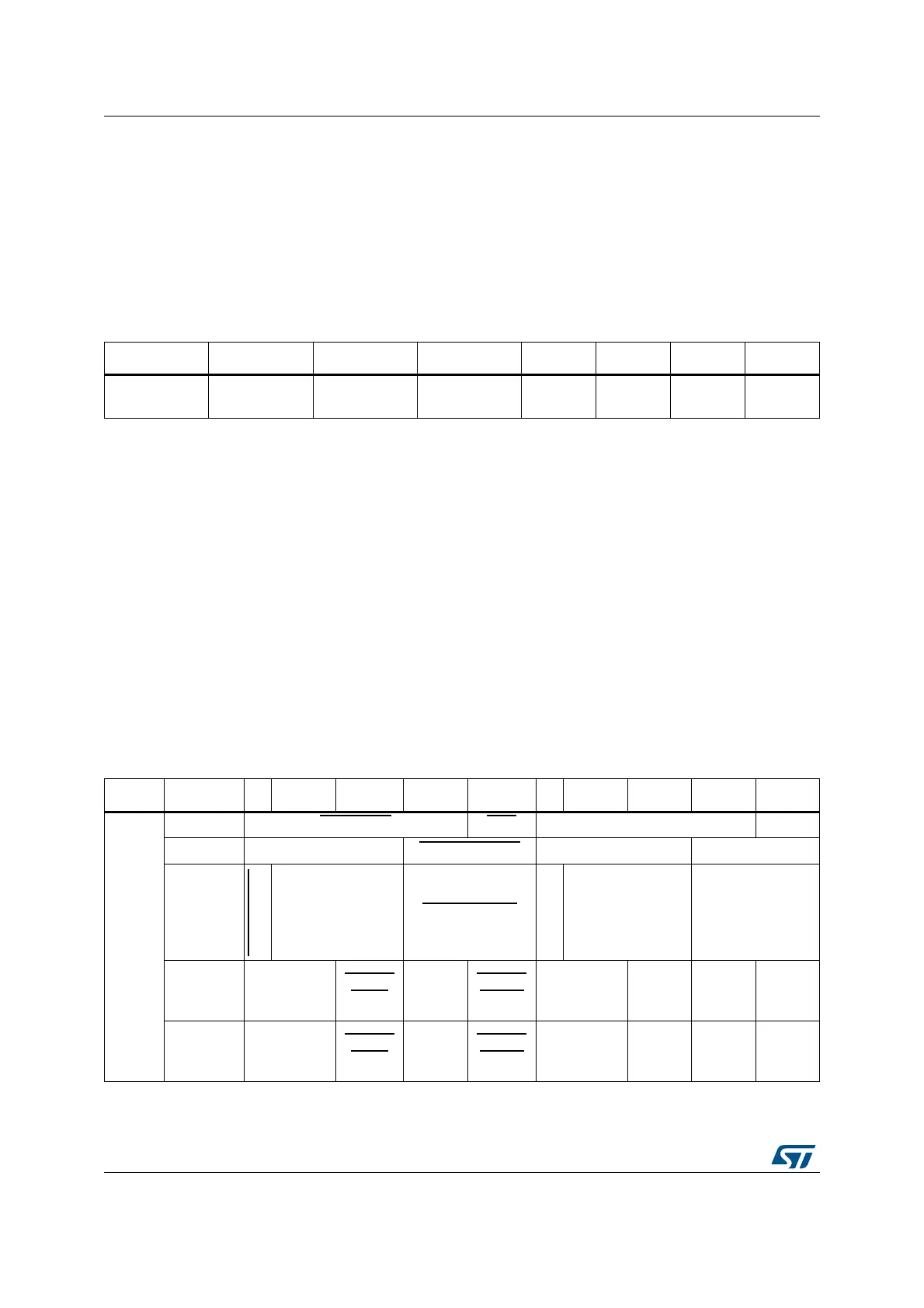
Table 9. Option byte format
63-24 23-16 15 -8 7-0 31-24 23-16 15 -8 7-0
Complemented
option byte 3
Complemented
option byte 2
Complemented
option byte 1
Complemented
option byte 0
Option
byte 3
Option
byte 2
Option
byte 1
Option
byte 0
Table 10. Option byte organization
BANK Address 63 [62:56] [55:48] [47:40] [39:32] 31 [30:24] [23:16] [15:8] [7:0]
Bank 1
1FFF7800 USER OPT
RDP USER OPT RDP
1FFF7808 Unused PCROP1_STRT
Unused PCROP1_STRT
1FFF7810
PCROP_RDP
Unused PCROP1_END
PCROP_RDP
Unused PCROP1_END
1FFF7818 Unused
WRP1A
_END
Unused
WRP1A
_STRT
Unused
WRP1A
_
END
Unused
WRP1A
_STRT
1FFF7820 Unused
WRP1B
_END
Unused
WRP1B
_STRT
Unused
WRP1B
_
END
Unused
WRP1B
_STRT