DocID024597 Rev 3 107/1693
RM0351 Embedded Flash memory (FLASH)
120
3.7.2 Flash Power-down key register (FLASH_PDKEYR)
Address offset: 0x04
Reset value: 0x0000 0000
Access: no wait state, word access
3.7.3 Flash key register (FLASH_KEYR)
Address offset: 0x08
Reset value: 0x0000 0000
Access: no wait state, word access
Bit 9 ICEN: Instruction cache enable
0: Instruction cache is disabled
1: Instruction cache is enabled
Bit 8 PRFTEN: Prefetch enable
0: Prefetch disabled
1: Prefetch enabled
Bits 7:3 Reserved, must be kept at reset value.
Bits 2:0 LATENCY[2:0]: Latency
These bits represent the ratio of the SYSCLK (system clock) period to the Flash
access time.
000: Zero wait state
001: One wait state
010: Two wait sates
011: Three wait sates
100: Four wait sates
others: reserved
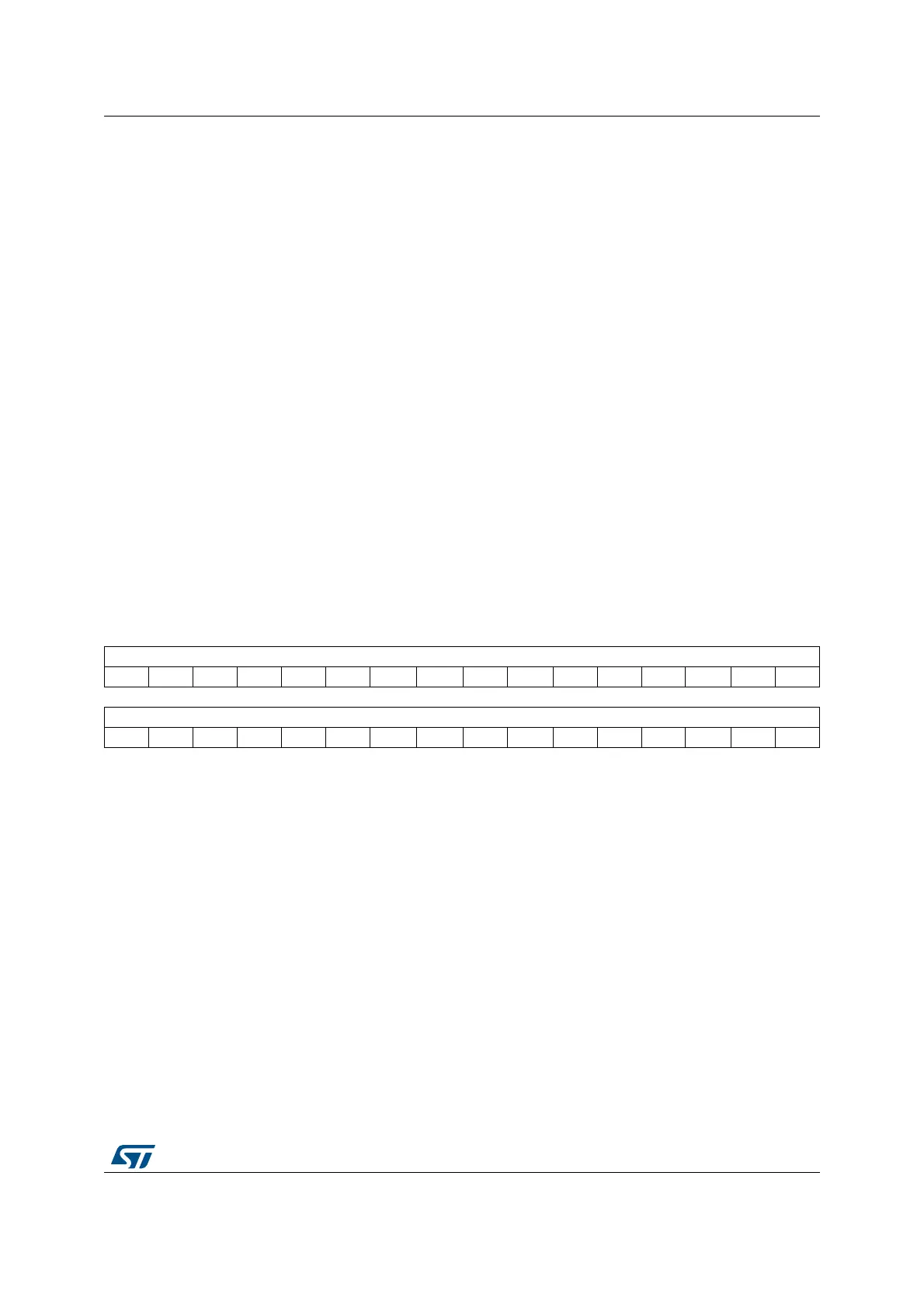
31 30 29 28 27 26 25 24 23 22 21 20 19 18 17 16
PDKEYR[31:16]
wwwwwww wwwwwww ww
15 14 13 12 11 10 9 8 7 6 5 4 3 2 1 0
PDKEYR[15:0]
wwwwwww wwwwwww ww
Bits 31:0 PDKEYR: Power-down in Run mode Flash key
The following values must be written consecutively to unlock the RUN_PD bit in
FLASH_ACR:
PDKEY1: 0x04152637
PDKEY2: 0xFAFBFCFD

 Loading...


