Advanced-control timers (TIM1/TIM8) RM0351
794/1693 DocID024597 Rev 3
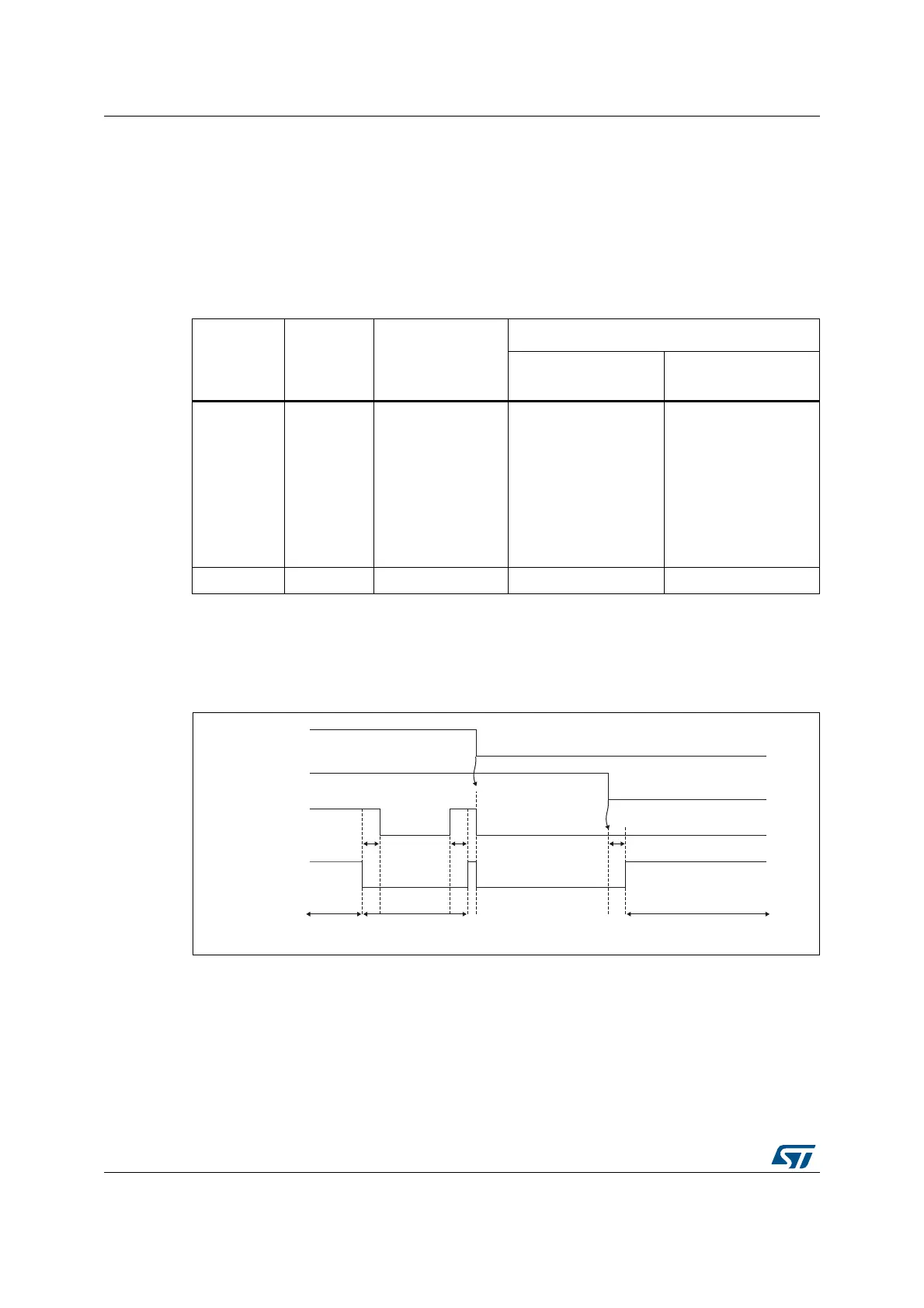
The two break inputs have different behaviors on timer outputs:
– The BRK input can either disable (inactive state) or force the PWM outputs to a
predefined safe state.
– BRK2 can only disable (inactive state) the PWM outputs.
The BRK has a higher priority than BRK2 input, as described in Table 146.
Note: BRK2 must only be used with OSSR = OSSI = 1.
Figure 234 gives an example of OCx and OCxN output behavior in case of active signals on
BRK and BRK2 inputs. In this case, both outputs have active high polarities (CCxP =
CCxNP = 0 in TIMx_CCER register).
Figure 234. PWM output state following BRK and BRK2 pins assertion (OSSI=1)
Table 146. Behavior of timer outputs versus BRK/BRK2 inputs
BRK BRK2
Timer outputs
state
Typical use case
OCxN output
(low side switches)
OCx output
(high side switches)
Active X
– Inactive then
forced output
state (after a
deadtime)
– Outputs disabled
if OSSI = 0
(control taken
over by GPIO
logic)
ON after deadtime
insertion
OFF
Inactive Active Inactive OFF OFF
D^ϯϰϭϬϲsϭ
Z<Ϯ
Z<
Kdž
/KƐƚĂƚĞ
ĞĂĚƚŝŵĞ ĞĂĚƚŝŵĞ
ĐƚŝǀĞ /ŶĂĐƚŝǀĞ /ĚůĞ

 Loading...


