DocID024597 Rev 3 1291/1685
RM0351 Serial peripheral interface (SPI)
1317
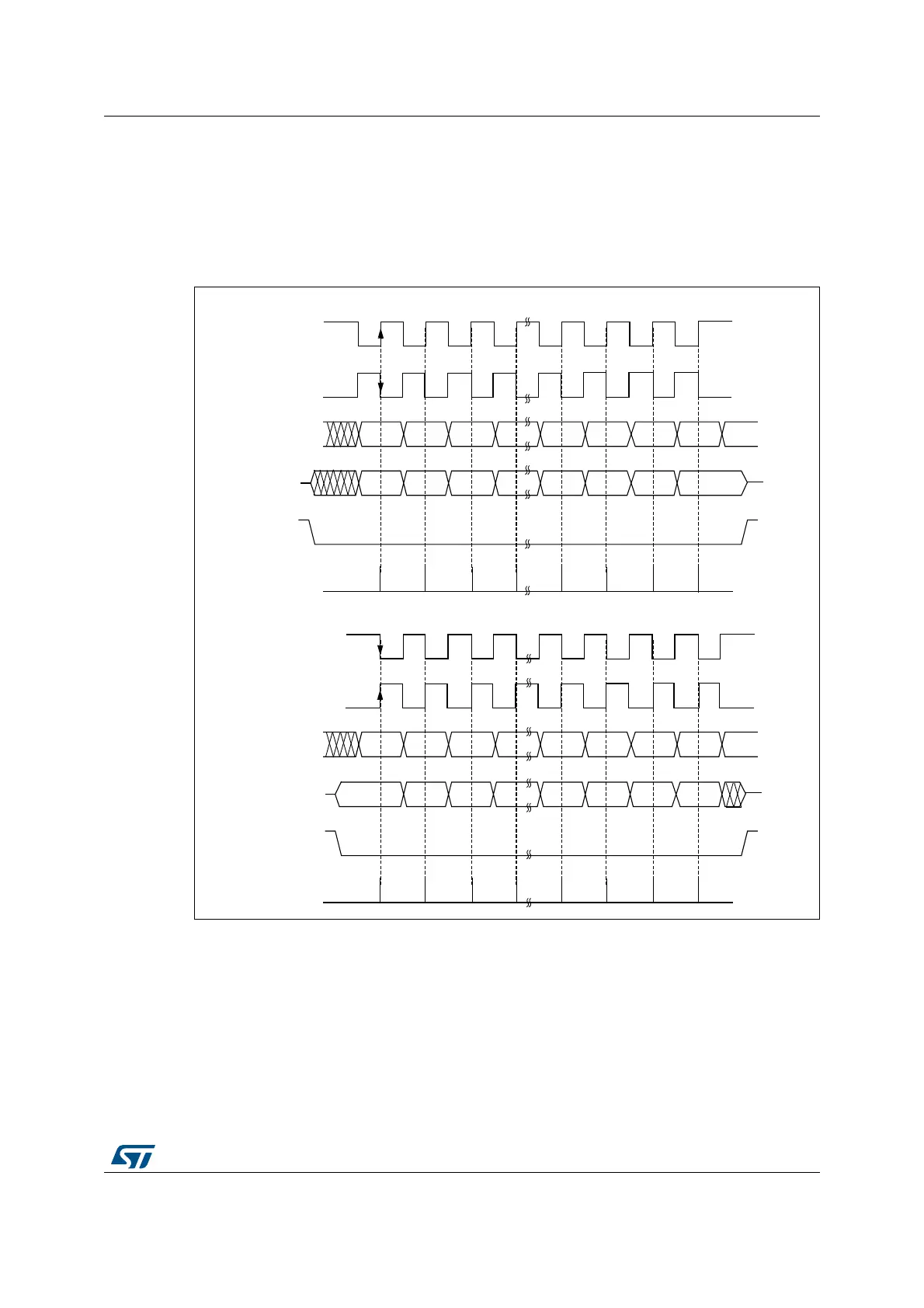
Figure 427, shows an SPI full-duplex transfer with the four combinations of the CPHA and
CPOL bits.
Note: Prior to changing the CPOL/CPHA bits the SPI must be disabled by resetting the SPE bit.
The idle state of SCK must correspond to the polarity selected in the SPIx_CR1 register (by
pulling up SCK if CPOL=1 or pulling down SCK if CPOL=0).
Figure 427. Data clock timing diagram
1. The order of data bits depends on LSBFIRST bit setting.
Data frame format
The SPI shift register can be set up to shift out MSB-first or LSB-first, depending on the
value of the LSBFIRST bit. The data frame size is chosen by using the DS bits. It can be set
from 4-bit up to 16-bit length and the setting applies for both transmission and reception.
Whatever the selected data frame size, read access to the FIFO must be aligned with the
FRXTH level. When the SPIx_DR register is accessed, data frames are always right-aligned
into either a byte (if the data fits into a byte) or a half-word (see Figure 428). During
communication, only bits within the data frame are clocked and transferred.
DLH
&3+$
&3+$
&32/
&32/
026,
0,62
166WRVODYH
&DSWXUHVWUREH
06%LW
06%LW
/6%LW
/6%LW
&32/
&32/
026,
0,62
166WRVODYH
&DSWXUHVWUREH
06%LW
06%LW
/6%LW
/6%LW

 Loading...


