DocID024597 Rev 3 517/1693
RM0351 Analog-to-digital converters (ADC)
540
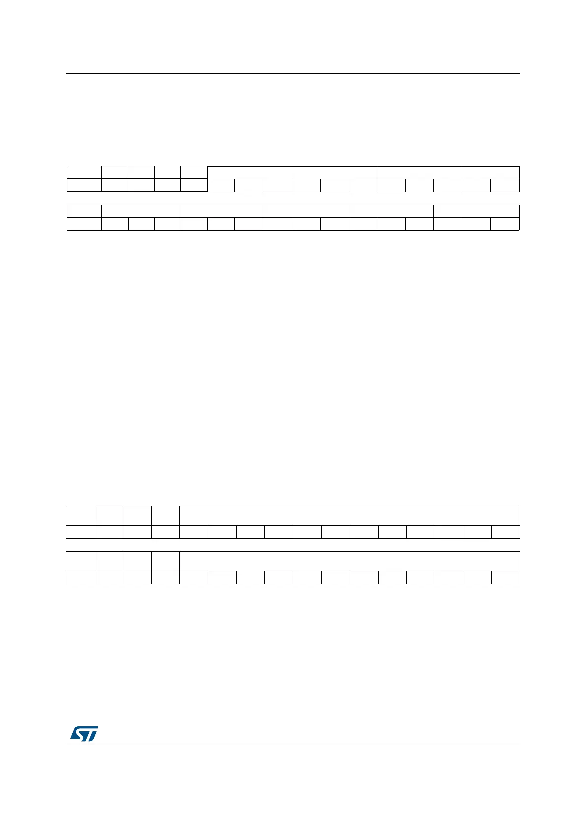
16.5.7 ADC sample time register 2 (ADCx_SMPR2)
Address offset: 0x18
Reset value: 0x0000 0000
16.5.8 ADC watchdog threshold register 1 (ADCx_TR1)
Address offset: 0x20
Reset value: 0x0FFF 0000
31 30 29 28 27 26 25 24 23 22 21 20 19 18 17 16
Res. Res. Res. Res. Res. SMP18[2:0] SMP17[2:0] SMP16[2:0] SMP15[2:1]
rw rw rw rw rw rw rw rw rw rw rw
15 14 13 12 11 10 9 8 7 6 5 4 3 2 1 0
SMP15_0 SMP14[2:0] SMP13[2:0] SMP12[2:0] SMP11[2:0] SMP10[2:0]
rw rw rw rw rw rw rw rw rw rw rw rw rw rw rw rw
Bits 31:27 Reserved, must be kept at reset value.
Bits 26:0 SMPx[2:0]: Channel x sampling time selection
These bits are written by software to select the sampling time individually for each channel.
During sampling cycles, the channel selection bits must remain unchanged.
000: 2.5 ADC clock cycles
001: 6.5 ADC clock cycles
010: 12.5 ADC clock cycles
011: 24.5 ADC clock cycles
100: 47.5 ADC clock cycles
101: 92.5 ADC clock cycles
110: 247.5 ADC clock cycles
111: 640.5 ADC clock cycles
Note: Software is allowed to write these bits only when ADSTART=0 and JADSTART=0
(which ensures that no conversion is ongoing).
31 30 29 28 27 26 25 24 23 22 21 20 19 18 17 16
Res. Res. Res. Res. HT1[11:0]
1514131211109876543210
Res. Res. Res. Res. LT1[11:0]
rw rw rw rw rw rw rw rw rw rw rw rw
Bits 31:28 Reserved, must be kept at reset value.

 Loading...


