Reset and clock control (RCC) RM0351
220/1693 DocID024597 Rev 3
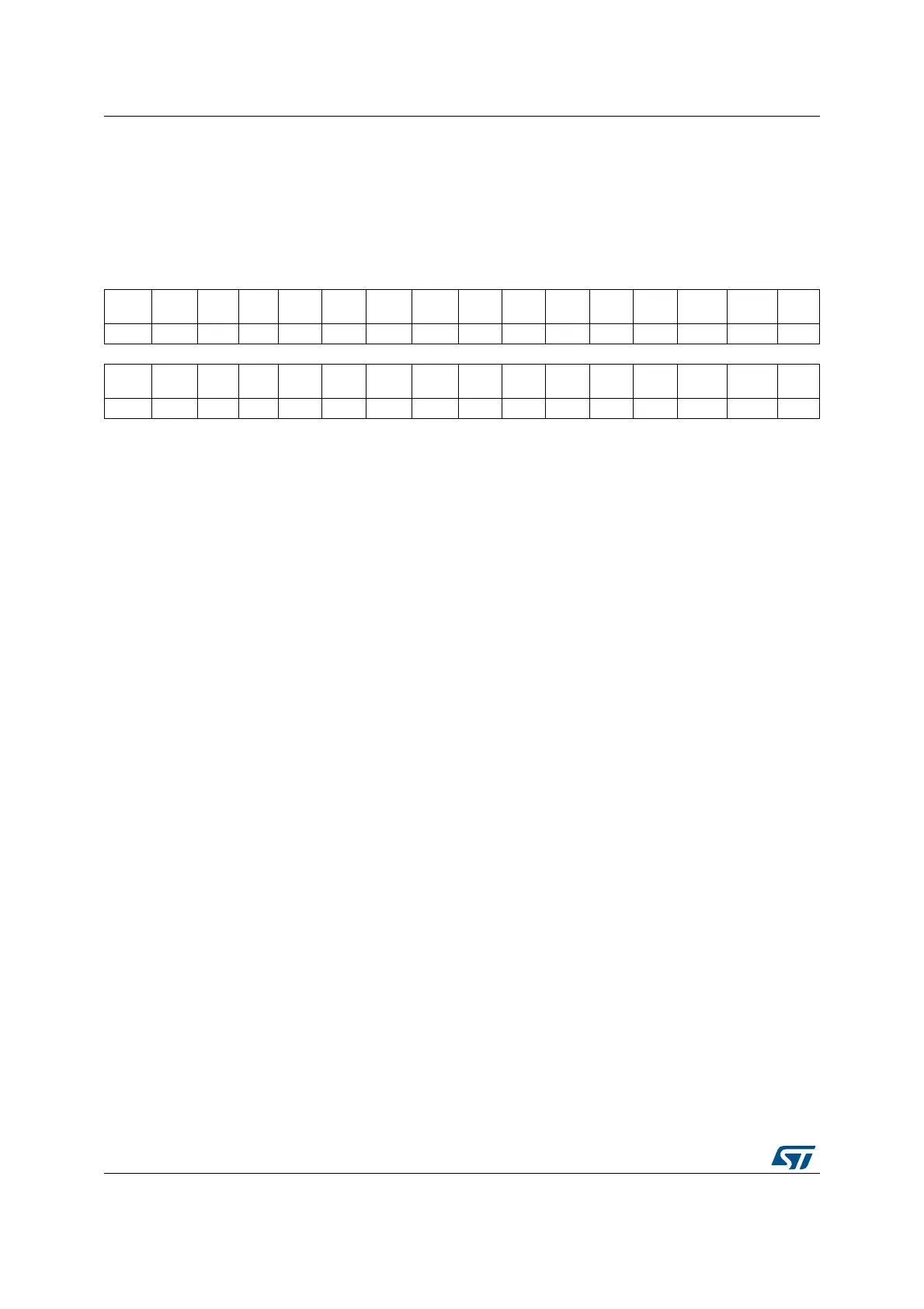
6.4.13 APB1 peripheral reset register 1 (RCC_APB1RSTR1)
Address offset: 0x38
Reset value: 0x0000 0000
Access: no wait state, word, half-word and byte access
31 30 29 28 27 26 25 24 23 22 21 20 19 18 17 16
LPTIM1
RST
OPAMP
RST
DAC1
RST
PWR
RST
Res. Res.
CAN1
RST
Res.
I2C3R
ST
I2C2
RST
I2C1
RST
UART5
RST
UART4
RST
USART3
RST
USART2
RST
Res.
rw rw rw rw rw rw rw rw rw rw rw rw
15 14 13 12 11 10 9 8 7 6 5 4 3 2 1 0
SPI3
RST
SPI2
RST
Res. Res. Res. Res.
LCD
RST
Res. Res. Res.
TIM7
RST
TIM6
RST
TIM5
RST
TIM4
RST
TIM3
RST
TIM2
RST
rw rw rw rw rw rw rw rw rw
Bit 31 LPTIM1RST: Low Power Timer 1 reset
Set and cleared by software.
0: No effect
1: Reset LPTIM1
Bit 30 OPAMPRST: OPAMP interface reset
Set and cleared by software.
0: No effect
1: Reset OPAMP interface
Bit 29 DAC1RST: DAC1 interface reset
Set and cleared by software.
0: No effect
1: Reset DAC1 interface
Bit 28 PWRRST: Power interface reset
Set and cleared by software.
0: No effect
1: Reset PWR
Bits 27:26 Reserved, must be kept at reset value.
Bit 25 CAN1RST: CAN1 reset
Set and reset by software.
0: No effect
1: Resets the CAN1
Bit 24 Reserved, must be kept at reset value
Bit 23 I2C3RST: I2C3 reset
Set and reset by software.
0: No effect
1: Resets I2C3
Bit 22 I2C2RST: I2C2 reset
Set and cleared by software.
0: No effect
1: Reset I2C2

 Loading...


