Inter-integrated circuit (I2C) interface RM0351
1160/1693 DocID024597 Rev 3
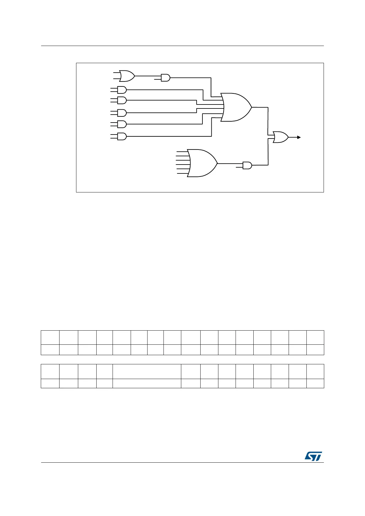
Figure 382. I2C interrupt mapping diagram
35.7 I2C registers
Refer to Section 1.1 on page 61 for a list of abbreviations used in register descriptions.
The peripheral registers are accessed by words (32-bit).
35.7.1 Control register 1 (I2C_CR1)
Address offset: 0x00
Reset value: 0x0000 0000
Access: No wait states, except if a write access occurs while a write access to this register is
ongoing. In this case, wait states are inserted in the second write access until the previous
one is completed. The latency of the second write access can be up to 2 x PCLK1 + 6 x
I2CCLK.
069
7&5
7;,6
7;,(
5;1(
5;,(
6723)
6723,(
$''5
$''5,(
1$&.)
1$&.,(
,&JOREDOLQWHUUXSW
%(55
295
$5/2
7,0(287
$/(57
3(&(55
7&,(
(55,(
7&
,&HUURULQWHUUXSW
,&HYHQWLQWHUUXSW
31 30 29 28 27 26 25 24 23 22 21 20 19 18 17 16
Res. Res. Res. Res. Res. Res. Res. Res. PECEN
ALERT
EN
SMBD
EN
SMBH
EN
GCEN
WUPE
N
NOSTR
ETCH
SBC
rw rw rw rw rw rw rw
15141312111098 7 6543210
RXDMA
EN
TXDMA
EN
Res.
ANF
OFF
DNF ERRIE TCIE
STOP
IE
NACK
IE
ADDR
IE
RXIE TXIE PE
rw rw rw rw rw rw rw rw rw rw rw rw
Bits 31:24 Reserved, must be kept at reset value.

 Loading...


