Liquid crystal display controller (LCD) RM0351
674/1693 DocID024597 Rev 3
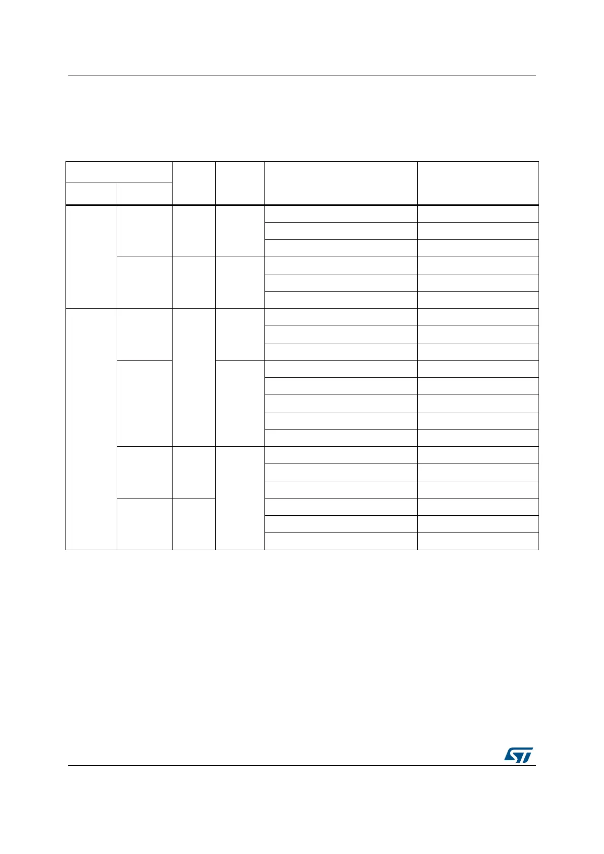
Summary of COM and SEG functions versus duty and remap
All the possible ways of multiplexing the COM and SEG functions are described in
Table 130. Figure 163 gives examples showing the signal connections to the external pins.
Table 130. Remapping capability
Configuration bits
CSP72
LQFP64
LQFP144
BGA132/
LQFP100
Output pin Function
DUTY MUX_SEG
1/8
0/1 - 40x8
SEG[43:40]/SEG[31:28]/COM[7:4] COM[7:4]
COM[3:0] COM[3:0]
SEG[39:0] SEG[39:0]
0/1 28x8 -
SEG[43:40]/SEG[31:28]/COM[7:4] COM[7:4]
COM[3:0] COM[3:0]
SEG[27:0] SEG[27:0]
1/4
0
-
44x4
COM[3:0] COM[3:0]
SEG[43:40]/SEG[31:28]/COM[7:4] SEG[43:40]
SEG[39:0] SEG[39:0]
140x4
COM[3:0] COM[3:0]
SEG[43:40]/SEG[31:28]/COM[7:4] SEG[31:28]
SEG[39:32] SEG[39:32]
SEG[31:28] not used
SEG[27:0] SEG[27:0]
0 28x4
-
COM[3:0] COM[3:0]
SEG[43:40]/SEG[31:28]/COM[7:4] not used
SEG[27:0] SEG[27:0]
1 32x4
COM[3:0] COM[3:0]
SEG[43:40]/SEG[31:28]/COM[7:4] SEG[31:28]
SEG[27:0] SEG[27:0]

 Loading...


