DocID024597 Rev 3 571/1693
RM0351 Digital-to-analog converter (DAC)
573
Note: These bits can be written only when the DAC channel is disabled and in normal operating
mode(when bit ENx=0 and bit CEN2x=0 in the DAC_CR register ). If ENx=1 or CENx=1 the
write operation is ignored.
17.5.20 DAC Sample and Hold refresh time register (DAC_SHRR)
Address offset: 0x4C
Reset value: 0x0001 0001
Note: These bits can be written only when the DAC channel is disabled and in normal operating
mode(when bit ENx=0 and bit CEN2x=0 in the DAC_CR register ). If ENx=1 or CENx=1 the
write operation is ignored.
Bits 31:26
Reserved, must be kept at reset value.
Bits 25:16 THOLD2[9:0]: DAC Channel 2 hold time (only valid in sample & hold mode).
Hold time= (THOLD[9:0] ) x T LSI
Bits 15:10 Reserved, must be kept at reset value.
Bits 9:0 THOLD1[9:0]: DAC Channel 1 hold Time (only valid in sample & hold mode)
Hold time= (THOLD[9:0] ) x T LSI
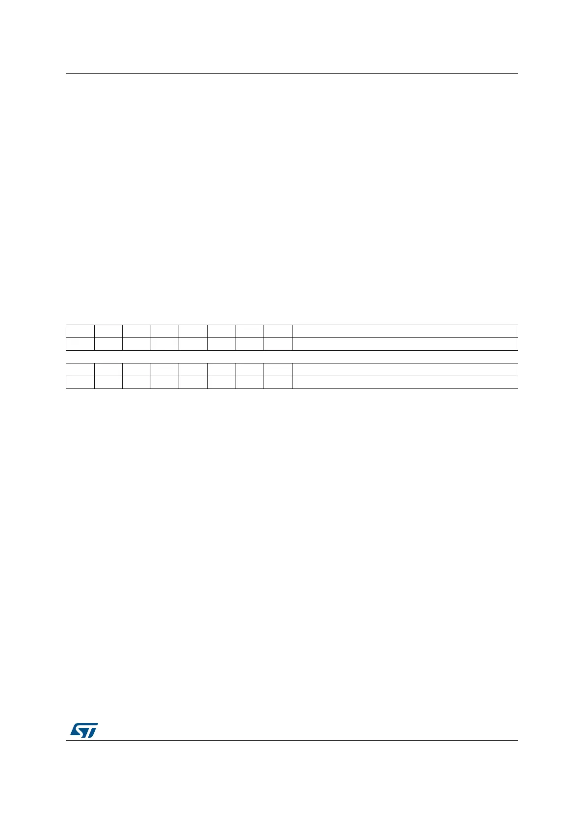
31 30 29 28 27 26 25 24 23 22 21 20 19 18 17 16
Res. Res. Res. Res. Res. Res. Res. Res. TREFRESH2[7:0]
rw
1514131211109876543210
Res. Res. Res. Res. Res. Res. Res. Res. TREFRESH1[7:0]
rw
Bits 31:24
Reserved, must be kept at reset value.
Bits 23:16 TREFRESH2[7:0]: DAC Channel 2 refresh Time (only valid in sample & hold mode)
Refresh time= (TREFRESH[7:0] ) x T LSI
Bits 15:8 Reserved, must be kept at reset value.
Bits 7:0 TREFRESH1[7:0]: DAC Channel 1 refresh Time (only valid in sample & hold mode)
Refresh time= (TREFRESH[7:0] ) x T LSI