DocID024597 Rev 3 95/1693
RM0351 Embedded Flash memory (FLASH)
120
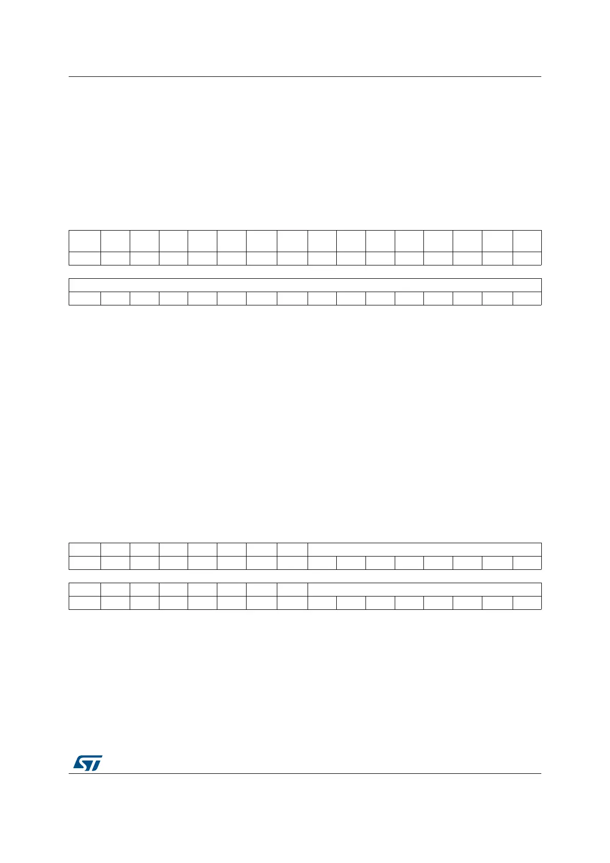
Bank 1 PCROP End address option bytes
Flash memory address: 0x1FFF 7810
ST production value: 0x0000 0000
Bank 1 WRP Area A address option bytes
Flash memory address: 0x1FFF 7818
ST production value: 0x0000 00FF
Bits 31:16 Not used
Bits 15:0 PCROP1_STRT: Bank 1 PCROP area start offset
PCROP1_STRT contains the first double-word of the bank 1 PCROP area.
31 30 29 28 27 26 25 24 23 22 21 20 19 18 17 16
PCROP
_RDP
Res. Res. Res. Res. Res. Res. Res. Res. Res. Res. Res. Res. Res. Res. Res.
r
15 14 13 12 11 10 9 8 7 6 5 4 3 2 1 0
PCROP1_END[15:0]
r rrrrr r r rrrrrr rr
Bit 31 PCROP_RDP: PCROP area preserved when RDP level decreased
This bit is set only. It is reset after a full mass erase due to a change of RDP
from Level 1 to Level 0.
0: PCROP area is not erased when the RDP level is decreased from Level 1 to
Level 0.
1: PCROP area is erased when the RDP level is decreased from Level 1 to
Level 0 (full mass erase).
Bits 30:16 Not used
Bits 15:0 PCROP1_END: Bank 1 PCROP area end offset
PCROP1_END contains the last double-word of the bank 1 PCROP area.
31 30 29 28 27 26 25 24 23 22 21 20 19 18 17 16
Res. Res. Res. Res. Res. Res. Res. Res. WRP1A_END[15:0]
rrrrrrrr
15 14 13 12 11 10 9 8 7 6 5 4 3 2 1 0
Res. Res. Res. Res. Res. Res. Res. Res. WRP1A_STRT[15:0]
rrrrrrrr
Bits 31:24 Not used
Bits 23:16 WRP1A_END: Bank 1 WRP first area “A” end offset
WRPA1_END contains the last page of the Bank 1 WRP first area.
Bits 15:8 Not used
Bits 7:0 WRP1A_STRT: Bank 1 WRP first area “A” start offset
WRPA1_STRT contains the first page of the Bank 1 WRP first area.
 Loading...


