45.4.3.3 After SCK Delay (t
ASC
)
The After SCK Delay is the length of time between the last edge of SCK and the negation
of PCS. See Figure 45-6 and Figure 45-7 for illustrations of the After SCK delay. The
PASC and ASC fields in the CTARx registers select the After SCK Delay by the formula
in the ASC field description. The following table shows an example of how to compute
the After SCK delay.
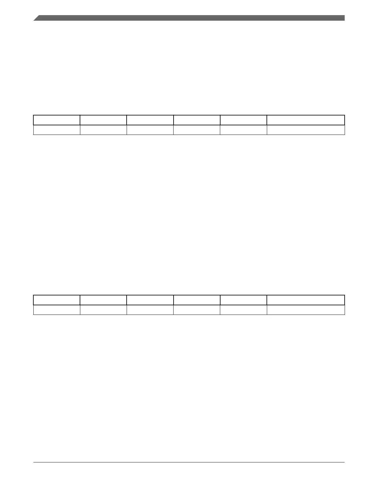
Table 45-7. After SCK Delay computation example
f
P
PASC Prescaler ASC Scaler After SCK Delay
100 MHz 0b01 3 0b0100 32 0.96 μs
NOTE
The clock frequency mentioned in the preceding table is given
as an example. Refer to the clocking chapter for the frequency
used to drive this module in the device.
45.4.3.4 Delay after Transfer (t
DT
)
The Delay after Transfer is the minimum time between negation of the PCS signal for a
frame and the assertion of the PCS signal for the next frame. See Figure 45-6 for an
illustration of the Delay after Transfer. The PDT and DT fields in the CTARx registers
select the Delay after Transfer by the formula in the DT field description. The following
table shows an example of how to compute the Delay after Transfer.
Table 45-8. Delay after Transfer computation example
f
P
PDT Prescaler DT Scaler Delay after Transfer
100 MHz 0b01 3 0b1110 32768 0.98 ms
NOTE
The clock frequency mentioned in the preceding table is given
as an example. Refer to the clocking chapter for the frequency
used to drive this module in the device.
When in Non-Continuous Clock mode the t
DT
delay is configured according to the
equation specified in the CTAR[DT] field description. When in Continuous Clock mode,
the delay is fixed at 1 SCK period.
Functional description
K22F Sub-Family Reference Manual, Rev. 4, 08/2016
1158 NXP Semiconductors

 Loading...