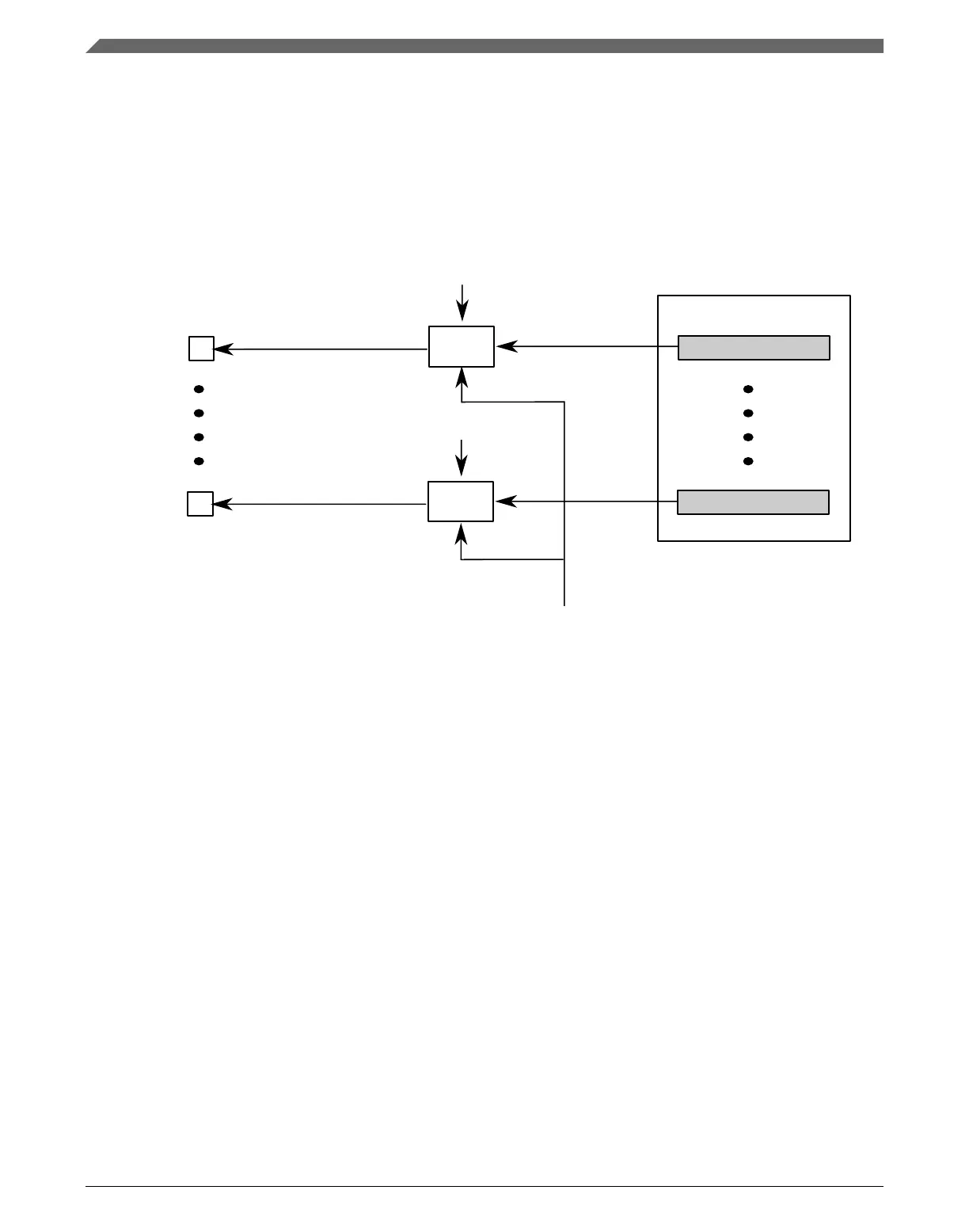
When FTM1_CH1 is used to modulate an FTM0 channel, then the user must configure
FTM1_CH1 to provide a signal that has a higher frequency than the modulated FTM0
channel output. Also it limits the use of the FTM1_CH0 function, as the FTM1_CH1 will
be programmed to provide a 50% duty PWM signal and limit the start and modulus
values for the free running counter. FTM2 has a similar restriction when FTM2_CH1 is
used for modulating an FTM3 channel.
FTM0
FTM0_CH7
&
SIM_SOPT8[FTM0CH7SRC]
CH7
FTM0_CH0
&
SIM_SOPT8[FTM0CH0SRC]
CH0
FTM1_CH1
Figure 3-40. FTM Output Modulation
3.8.2.10
FTM output triggers for other modules
FTM output triggers can be selected as input triggers for the PDB and ADC modules. See
PDB Instantiation and ADC triggers.
3.8.2.11
FTM Global Time Base
This chip provides the optional FTM global time base feature (see Global time base
(GTB)).
FTM0 provides the only source for the FTM global time base. The other FTM modules
can share the time base as shown in the following figure:
Timers
K22F Sub-Family Reference Manual, Rev. 4, 08/2016
116 NXP Semiconductors

 Loading...