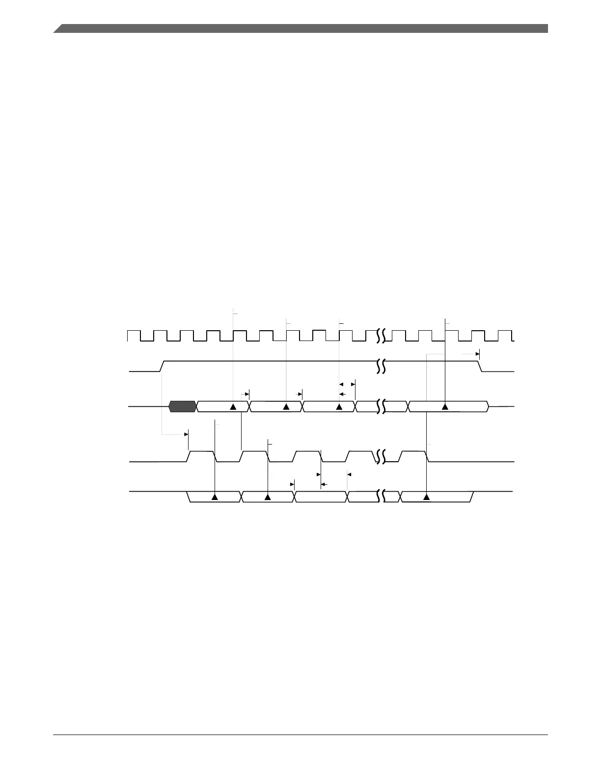
signal on the odd numbered SCK edges starting with the third SCK edge. The slave
samples the last bit on the last edge of the SCK. The master samples the last slave SOUT
bit one half SCK cycle after the last edge of SCK. No clock edge will be visible on the
master SCK pin during the sampling of the last bit. The SCK to PCS delay and the
After SCK delay must be greater or equal to half of the SCK period.
NOTE
When MTFE=1 with continuous SCK enabled (MCR
[CONT_SCKE] =1) in master mode, configure
CTAR[LSBFE]=0 for correct operations while receiving
unequal length frames. If PUSHR[CONT] is also set for back to
back frame transfer, also configure the frame size of the first
frame as less than or equal to the frame size of the next frame.
In this scenario, make sure that for all received frames, the bits
are read equal to their respective frame sizes and any extra bits
during POP operation are masked.
sys clk
PCS
SIN
SCK
SOUT
D1D0 D2 Dn
D0 D1 D2 Dn
Tcsc
Tvd_sl
Tsu_ms
Thd_ms
Tasc
Slave samples SOUT
Thd_sl
Tsu_sl
2n+2
2n+1
8
7
6
5
4
3
2
1
DSPI samples SIN
Figure 45-11. DSPI Modified Transfer Format (MTFE=1, CPHA=1, f
sck
= f
sys
/2)
Functional description
K22F Sub-Family Reference Manual, Rev. 4, 08/2016
1166 NXP Semiconductors

 Loading...