sys clk
PCS
SIN
SOUT
SCK
DSPI samples SIN
Tvd_sl
Thd_ms
Tasc
Tcsc
Slave samples SOUT
D0
D1
D2
Dn
Tsu_sl
Thd_sl
D0
D1
D2
Tsu_ms
Dn
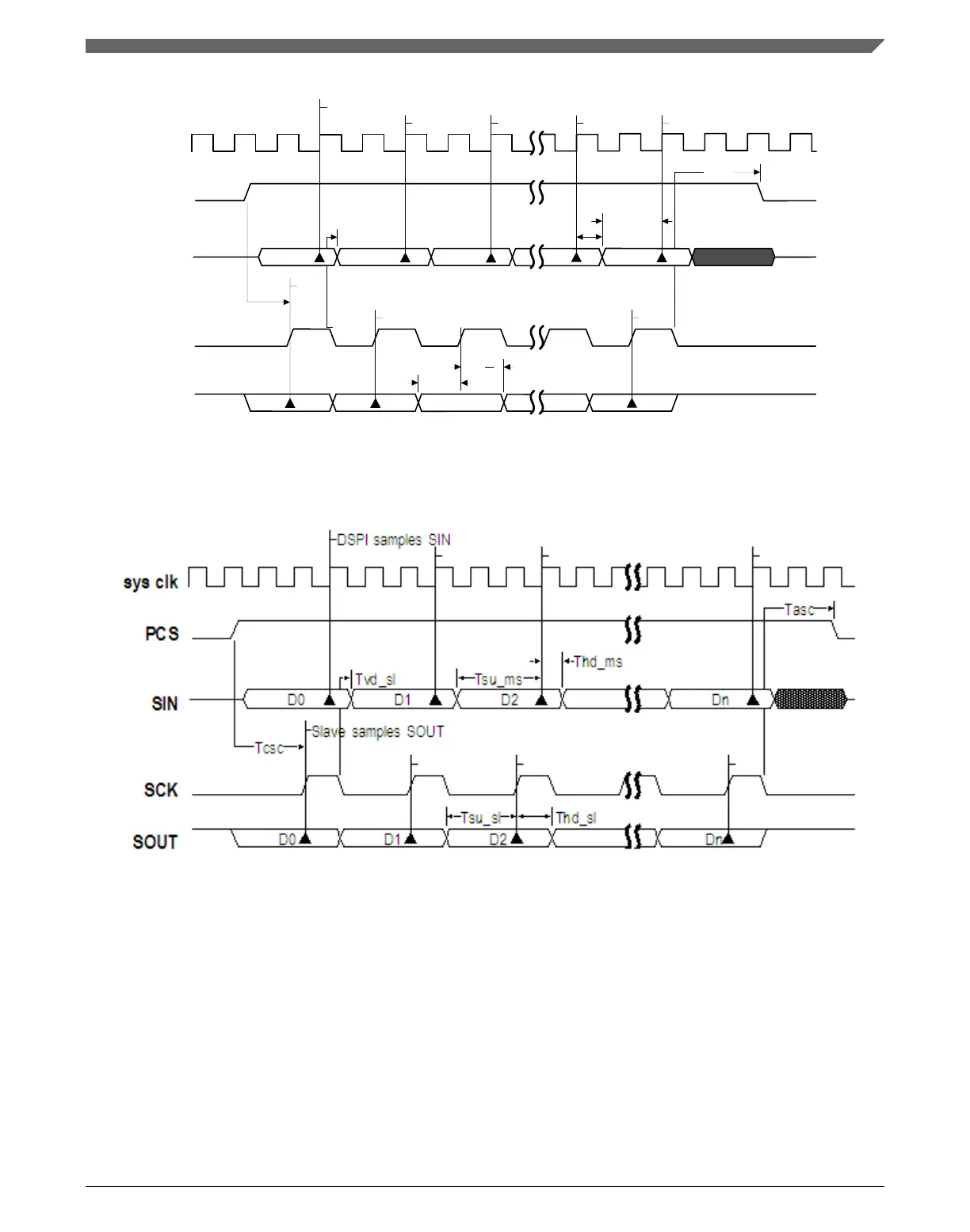
Figure 45-9. DSPI Modified Transfer Format (MTFE=1, CPHA=0, f
sck
= f
sys
/2)
Figure 45-10. DSPI Modified Transfer Format (MTFE=1, CPHA=0, f
sck
= f
sys
/3)
45.4.4.4
Modified SPI Transfer Format (MTFE = 1, CPHA = 1)
The following figures show the Modified Transfer Format for CPHA = 1. Only the
condition, where CPOL = 0 is shown. At the start of a transfer the DSPI asserts the PCS
signal to the slave device. After the PCS to SCK delay has elapsed the master and the
slave put data on their SOUT pins at the first edge of SCK . The slave samples the master
SOUT signal on the even numbered edges of SCK. The master samples the slave SOUT
Chapter 45 Serial Peripheral Interface (SPI)
K22F Sub-Family Reference Manual, Rev. 4, 08/2016
NXP Semiconductors 1165

 Loading...