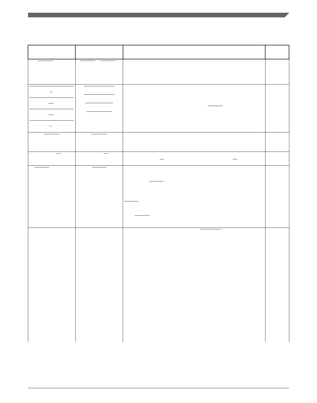
Table 10-10. FlexBus Signal Descriptions
(continued)
Chip signal name Module signal
name
Description I/O
FB_CS[5:0]
2
FB_CS5–FB_CS0 General Purpose Chip-Selects—Indicate which external memory or
peripheral is selected. A particular chip-select is asserted when the
transfer address is within the external memory's or peripheral's
address space, as defined in CSAR[BA] and CSMR[BAM].
O
FB_BE31_24_BLS7_
0,
FB_BE23_16_BLS15
_8,
FB_BE15_8_BLS23_
16,
FB_BE7_0_BLS31_2
4
3
FB_BE_31_24
FB_BE_23_16
FB_BE_15_8
FB_BE_7_0
Byte Enables—Indicate that data is to be latched or driven onto a
specific byte lane of the data bus. CSCR[BEM] determines if these
signals are asserted on reads and writes or on writes only.
For external SRAM or flash devices, the FB_BE outputs should be
connected to individual byte strobe signals.
O
FB_OE FB_OE Output Enable—Sent to the external memory or peripheral to
enable a read transfer. This signal is asserted during read accesses
only when a chip-select matches the current address decode.
O
FB_R W FB_R/W Read/Write—Indicates whether the current bus operation is a read
operation (FB_R/W high) or a write operation (FB_R/W low).
O
FB_TS/ FB_ALE FB_TS Transfer Start—Indicates that the chip has begun a bus transaction
and that the address and attributes are valid.
An inverted FB_TS is available as an address latch enable
(FB_ALE), which indicates when the address is being driven on the
FB_AD bus.
FB_TS/FB_ALE is asserted for one bus clock cycle.
The chip can extend this signal until the first positive clock edge
after FB_CS asserts. See CSCR[EXTS] and Extended Transfer
Start/Address Latch Enable.
O
FB_TSIZ[1:0] FB_TSIZ1–FB_TSIZ0 Transfer Size—Indicates (along with FB_TBST) the data transfer
size of the current bus operation. The interface supports 8-, 16-,
and 32-bit operand transfers and allows accesses to 8-, 16-, and
32-bit data ports.
• 00b = 4 bytes
• 01b = 1 byte
• 10b = 2 bytes
• 11b = 16 bytes (line)
For misaligned transfers, FB_TSIZ1–FB_TSIZ0 indicate the size of
each transfer. For example, if a 32-bit access through a 32-bit port
device occurs at a misaligned offset of 1h, 8 bits are transferred first
(FB_TSIZ1–FB_TSIZ0 = 01b), 16 bits are transferred next at offset
2h (FB_TSIZ1–FB_TSIZ0 = 10b), and the final 8 bits are transferred
at offset 4h (FB_TSIZ1–FB_TSIZ0 = 01b).
For aligned transfers larger than the port size, FB_TSIZ1–
FB_TSIZ0 behave as follows:
O
Table continues on the next page...
Chapter 10 Signal Multiplexing and Signal Descriptions
K22F Sub-Family Reference Manual, Rev. 4, 08/2016
NXP Semiconductors 231

 Loading...