Table 28-4. Flash Protection Ranges (continued)
SAn and XAn
Bit
Protected Segment Address Range Segment Size (Fraction
of total Flash)
0 0x0_0000_0000 – (Flash_size/64-1) 1/64
1 (Flash_size/64) – 2*(Flash_size/64-1) 1/64
........
63 63*(Flash_size/64) – 62*(Flash_size/64-1) 1/64
32 Segment Encodings
0 0x0_0000_0000 – (Flash_size/32-1) 1/32
1 (Flash_size/32) – 2*(Flash_size/32-1) 1/32
........
31 31*(Flash_size/32) – 30*(Flash_size/32-1) 1/32
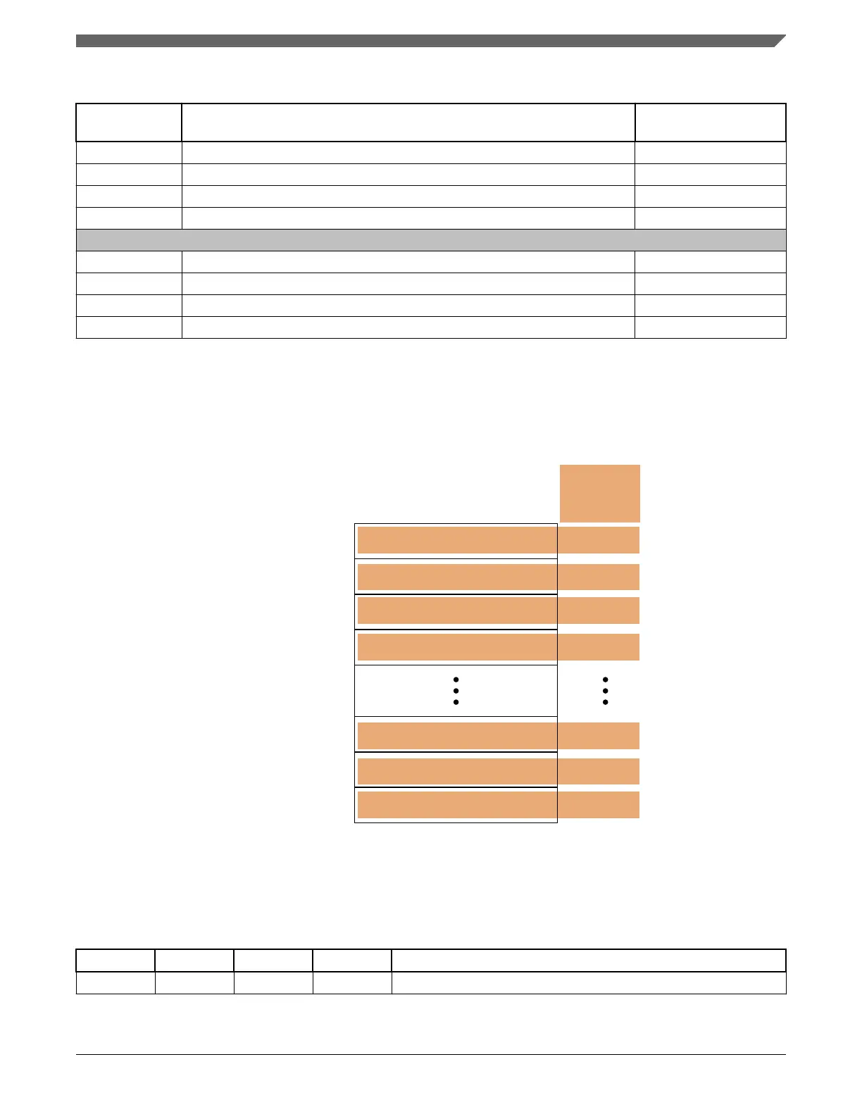
Individual segments within the flash memory can be independently protected from user
access and data access. Protection is controlled by the individual bits within the x_SACC
and x_XACC registers, as shown in the next figure.
Program flash size / 64
Program flash size / 64
Program flash size / 64
Program flash size / 64
Program flash size / 64
Program flash size / 64
Program flash size / 64
SA0/XA0
0x0000_0000
SA1/XA1
SA2/XA2
SA3/XA3
SA61/XA61
SA63/XA63
SA62/XA62
Program flash
Last program flash address
Access
Control bits
(SAn/XAn)
64 segments
Figure 28-1. Program flash protection (64 segments)
28.5.4.2.1
Interface Signals
Table 28-5. Interface Signals
Signal Width From To Description
xacc 64 or 32 FMU Platform Direct xacc (execute-only access control) register
Table continues on the next page...
Chapter 28 Flash Memory Controller (FMC)
K22F Sub-Family Reference Manual, Rev. 4, 08/2016
NXP Semiconductors 623

 Loading...