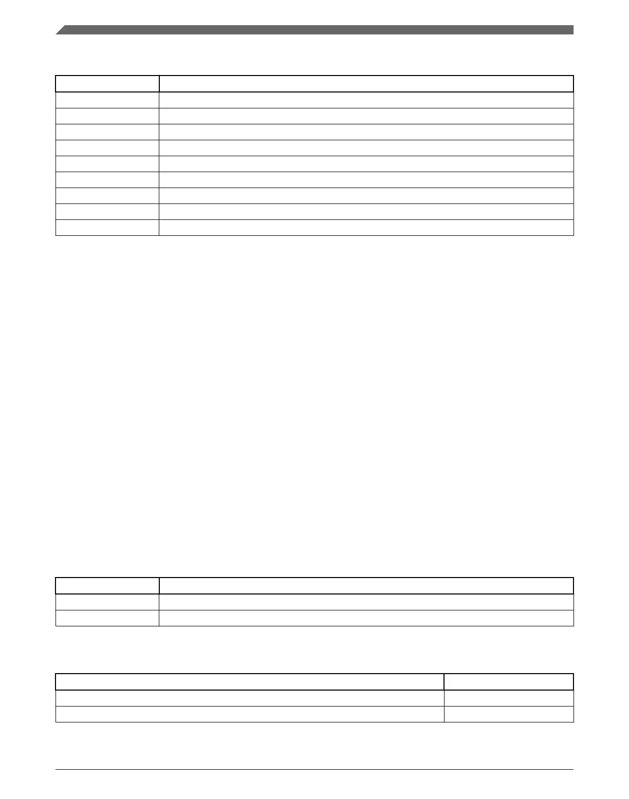
Table 29-10. Program Check Command FCCOB Requirements
FCCOB Number FCCOB Contents [7:0]
0 0x02 (PGMCHK)
1 Flash address [23:16]
2 Flash address [15:8]
3 Flash address [7:0]
1
4 Margin Choice
8 Byte 0 expected data
9 Byte 1 expected data
A Byte 2 expected data
B Byte 3 expected data
1. Must be longword aligned (Flash address [1:0] = 00).
Upon clearing CCIF to launch the Program Check command, the flash memory module
sets the read margin for 1s according to Table 29-11, reads the specified longword, and
compares the actual read data to the expected data provided by the FCCOB. If the
comparison at margin-1 fails, FSTAT[MGSTAT0] is set.
The flash memory module then sets the read margin for 0s, re-reads, and compares again.
If the comparison at margin-0 fails, FSTAT[MGSTAT0] is set. FSTAT[CCIF] is set after
the Program Check operation completes.
The supplied address must be longword aligned (the lowest two bits of the byte address
must be 00):
• Byte 3 data is written to the supplied byte address ('start'),
• Byte 2 data is programmed to byte address start+0b01,
• Byte 1 data is programmed to byte address start+0b10,
• Byte 0 data is programmed to byte address start+0b11.
NOTE
See the description of margin reads, Margin Read Commands
Table 29-11. Margin Level Choices for Program Check
Read Margin Choice Margin Level Description
0x01 Read at 'User' margin-1 and 'User' margin-0
0x02 Read at 'Factory' margin-1 and 'Factory' margin-0
Table 29-12. Program Check Command Error Handling
Error Condition Error Bit
Command not available in current mode/security FSTAT[ACCERR]
An invalid flash address is supplied FSTAT[ACCERR]
Table continues on the next page...
Functional Description
K22F Sub-Family Reference Manual, Rev. 4, 08/2016
662 NXP Semiconductors

 Loading...