Any write to the OUTMASK register, stores the value in its write buffer. The register is
updated with the value of its write buffer according to PWM synchronization.
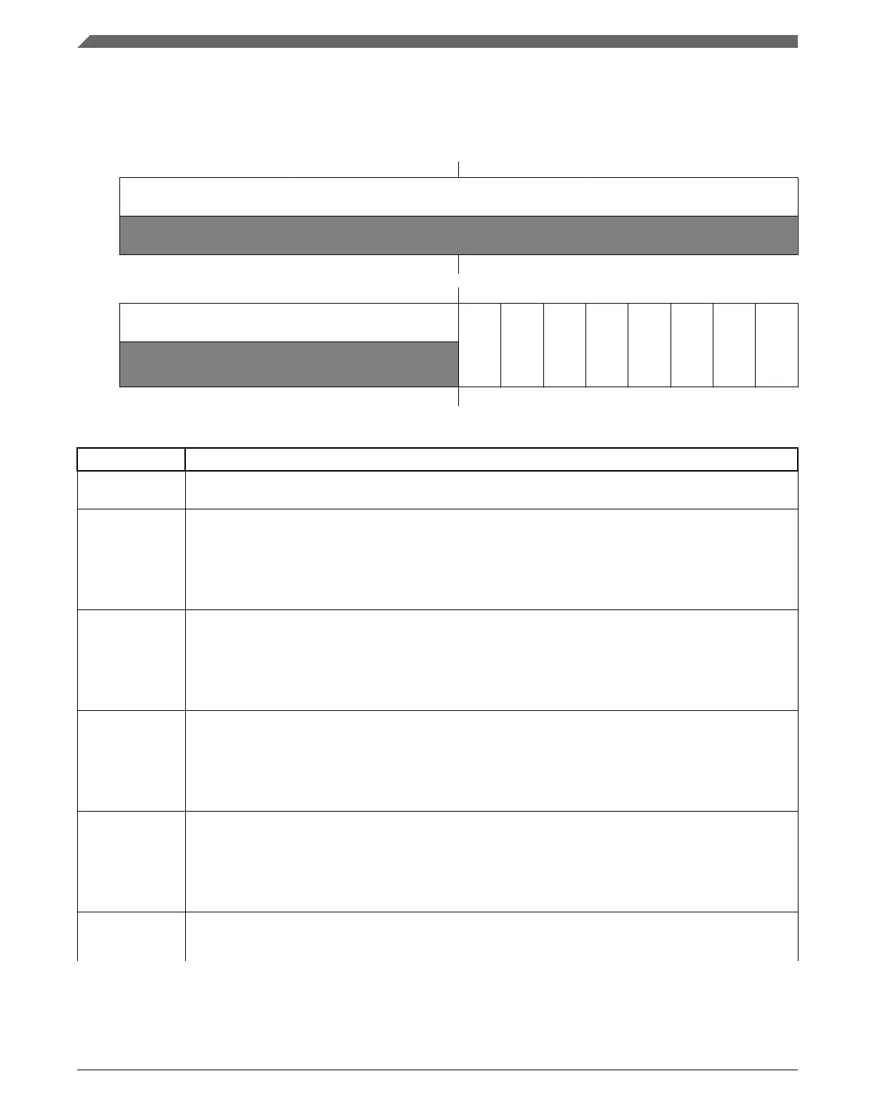
Address: Base address + 60h offset
Bit 31 30 29 28 27 26 25 24 23 22 21 20 19 18 17 16
R
0
W
Reset
0 0 0 0 0 0 0 0 0 0 0 0 0 0 0 0
Bit
15 14 13 12 11 10 9 8 7 6 5 4 3 2 1 0
R
0
CH7OM
CH6OM
CH5OM
CH4OM
CH3OM
CH2OM
CH1OM
CH0OM
W
Reset
0 0 0 0 0 0 0 0 0 0 0 0 0 0 0 0
FTMx_OUTMASK field descriptions
Field Description
31–8
Reserved
This field is reserved.
This read-only field is reserved and always has the value 0.
7
CH7OM
Channel 7 Output Mask
Defines if the channel output is masked or unmasked.
0 Channel output is not masked. It continues to operate normally.
1 Channel output is masked. It is forced to its inactive state.
6
CH6OM
Channel 6 Output Mask
Defines if the channel output is masked or unmasked.
0 Channel output is not masked. It continues to operate normally.
1 Channel output is masked. It is forced to its inactive state.
5
CH5OM
Channel 5 Output Mask
Defines if the channel output is masked or unmasked.
0 Channel output is not masked. It continues to operate normally.
1 Channel output is masked. It is forced to its inactive state.
4
CH4OM
Channel 4 Output Mask
Defines if the channel output is masked or unmasked.
0 Channel output is not masked. It continues to operate normally.
1 Channel output is masked. It is forced to its inactive state.
3
CH3OM
Channel 3 Output Mask
Defines if the channel output is masked or unmasked.
Table continues on the next page...
Memory map and register definition
K22F Sub-Family Reference Manual, Rev. 4, 08/2016
918 NXP Semiconductors

 Loading...