UM10360 All information provided in this document is subject to legal disclaimers. © NXP B.V. 2013. All rights reserved.
User manual Rev. 3 — 19 December 2013 404 of 841
NXP Semiconductors
UM10360
Chapter 17: LPC176x/5x SPI
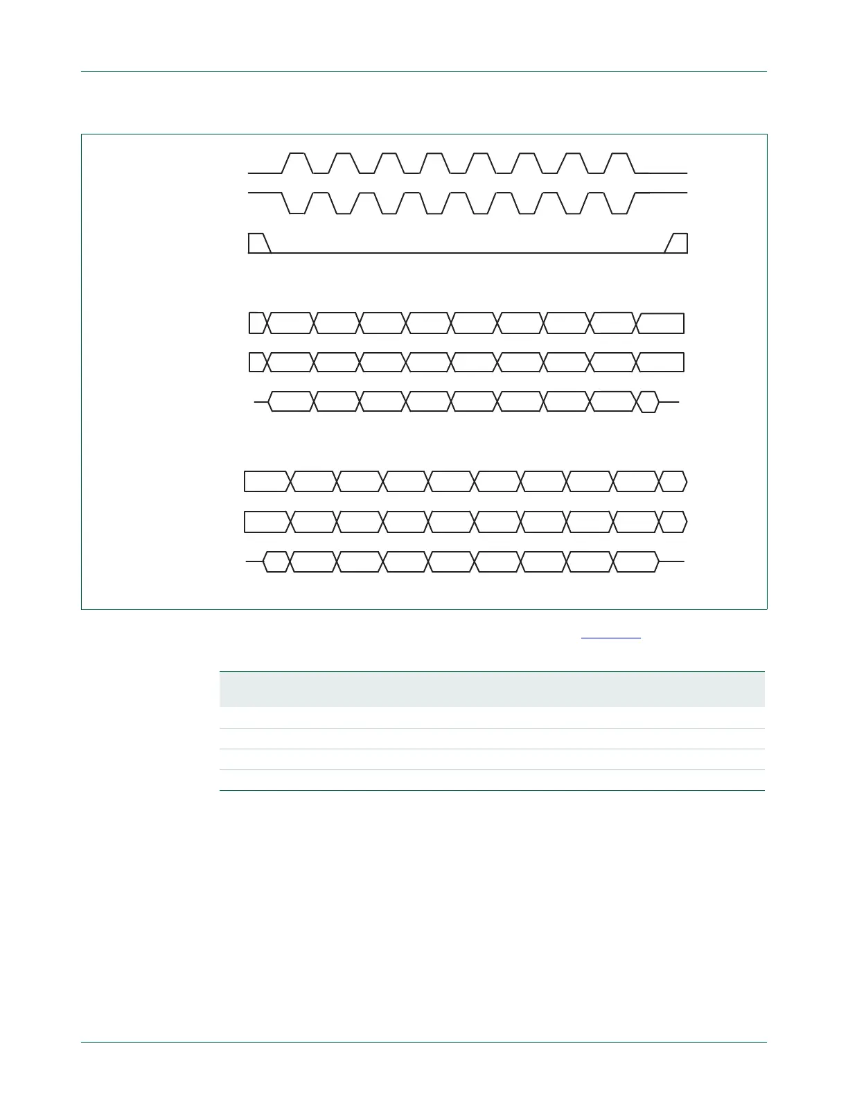
The data and clock phase relationships are summarized in Table 359.
The definition of when a transfer starts and stops is dependent on whether a device is a
master or a slave, and the setting of the CPHA variable.
When a device is a master, the start of a transfer is indicated by the master having a byte
of data that is ready to be transmitted. At this point, the master can activate the clock, and
begin the transfer. The transfer ends when the last clock cycle of the transfer is complete.
When a device is a slave and CPHA is set to 0, the transfer starts when the SSEL signal
goes active, and ends when SSEL goes inactive. When a device is a slave, and CPHA is
set to 1, the transfer starts on the first clock edge when the slave is selected, and ends on
the last clock edge where data is sampled.
Fig 74. SPI data transfer format (CPHA = 0 and CPHA = 1)
MISO (CPHA = 1)
MOSI (CPHA = 1)
Cycle # CPHA = 1
CPHA = 1
MISO (CPHA = 0)
MOSI (CPHA = 0)
Cycle # CPHA = 0
CPHA = 0
SSEL
SCK (CPOL = 1)
SCK (CPOL = 0)
123 87654
BIT 1 BIT 2 BIT 3 BIT 8BIT 7BIT 6BIT 5BIT 4
BIT 1 BIT 2 BIT 3 BIT 8BIT 7BIT 6BIT 5BIT 4
123 87654
BIT 1 BIT 2 BIT 3 BIT 8BIT 7BIT 6BIT 5BIT 4
BIT 1 BIT 2 BIT 3 BIT 8BIT 7BIT 6BIT 5BIT 4
Table 359. SPI Data To Clock Phase Relationship
CPOL and CPHA
settings
When the first data bit is
driven
When all other data
bits are driven
When data is
sampled
CPOL = 0, CPHA = 0 Prior to first SCK rising edge SCK falling edge SCK rising edge
CPOL = 0, CPHA = 1 First SCK rising edge SCK rising edge SCK falling edge
CPOL = 1, CPHA = 0 Prior to first SCK falling edge SCK rising edge SCK falling edge
CPOL = 1, CPHA = 1 First SCK falling edge SCK falling edge SCK rising edge

 Loading...


