UM10360 All information provided in this document is subject to legal disclaimers. © NXP B.V. 2013. All rights reserved.
User manual Rev. 3 — 19 December 2013 46 of 841
NXP Semiconductors
UM10360
Chapter 4: LPC176x/5x Clocking and power control
Example 3
Assumptions:
• The USB interface will not be used in the application, or will be clocked by PLL1.
• The desired CPU rate is 72 MHz
• The 32.768 kHz RTC clock source will be used as the system clock source
Calculations:
M = (F
CCO
N) / (2 F
IN
)
The smallest integer multiple of the desired CPU clock rate that is within the PLL0
operating range is 288 MHz (4 72 MHz).
Using the equation above and assuming that N = 1, M = ((288 10
6
) 1) / (2 32,768) =
4,394.53125. This is not an integer, so the CPU frequency will not be exactly 72 MHz with
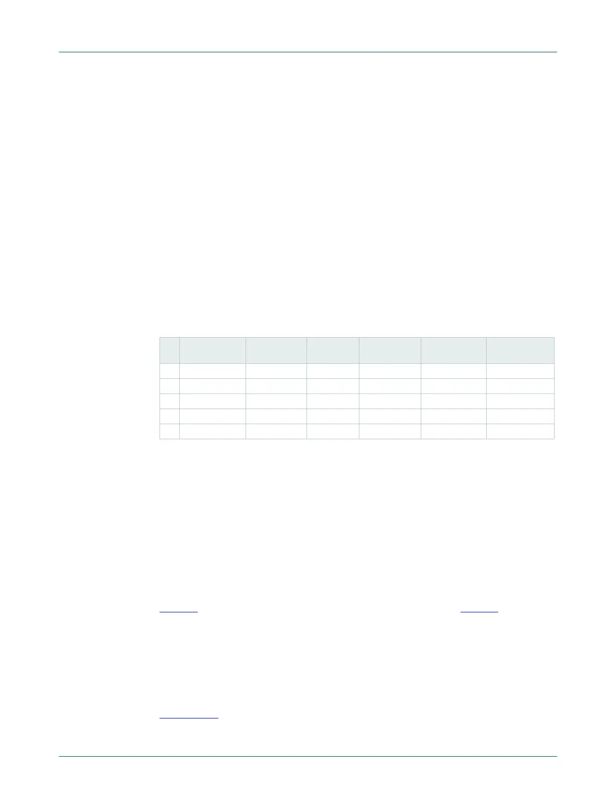
this setting. Since this example is less obvious, it may be useful to make a table of
possibilities for different values of N (see below).
Beyond N = 5, the value of M is out of range or not supported, so the table stops at that
point. In the third column of the table, the calculated M value is rounded to the nearest
integer. If this results in CCLK being above the maximum operating frequency, it is
allowed if it is not more than 1/2 above the maximum frequency.
In general, larger values of F
REF
result in a more stable PLL when the input clock is a low
frequency. Even the first table entry shows a very small error of just over 1 hundredth of a
percent, or 107 parts per million (ppm). If that is not accurate enough in the application,
the second case gives a much smaller error of 7 ppm. There are no allowed combinations
that give a smaller error than that.
Remember that when a frequency below about 1 MHz is used as the PLL0 clock source,
not all multiplier values are available. As it turns out, all of the rounded M values found in
Table 28
of this example are supported, which may be confirmed in Table 26. If PLL0
calculations suggest use of unsupported multiplier values, those values must be
disregarded and other values examined to find the best fit.
The value written to PLL0CFG for the second table entry would be 0x12254
(N - 1 = 1 = 0x1; M - 1 = 8788 = 0x2254).
The PLL output must be further divided in order to produce the CPU clock. This is
accomplished using a separate divider that is described later in this chapter, see
Section 4.7.1
.
Table 28. Potential values for PLL example
N M M Rounded F
REF
in Hz
(F
IN
/ N)
F
CCO
in MHz
(F
REF
x M)
CCLK in MHz
(F
CCO
/ 4)
Error
(CCLK-72) / 72
1 4394.53125 4395 32768 288.0307 72.0077 0.0107
2 8789.0625 8789 16384 287.9980 71.9995 -0.0007
3 13183.59375 13184 10922.67 288.0089 72.0022 0.0031
4 17578.125 17578 8192 287.9980 71.9995 -0.0007
5 21972.65625 21973 6553.6 288.0045 72.0011 0.0016

 Loading...


