RM0444 Rev 5 101/1390
RM0444 Embedded Flash memory (FLASH)
118
3.7.2 FLASH key register (FLASH_KEYR)
Address offset: 0x008
Reset value: 0x0000 0000
s
3.7.3 FLASH option key register (FLASH_OPTKEYR)
Address offset: 0x00C
Reset value: 0x0000 0000
s
Bit 8 PRFTEN: CPU Prefetch enable
0: CPU Prefetch disabled
1: CPU Prefetch enabled
Bits 7:3 Reserved, must be kept at reset value.
Bits 2:0 LATENCY[2:0]: Flash memory access latency
The value in this bitfield represents the ratio of the HCLK clock period to the Flash memory
access time.
000: Zero wait states
001: One wait state
010: Two wait states
Others: Reserved
A a new write into the bitfield becomes effective when it returns the same value upon read.
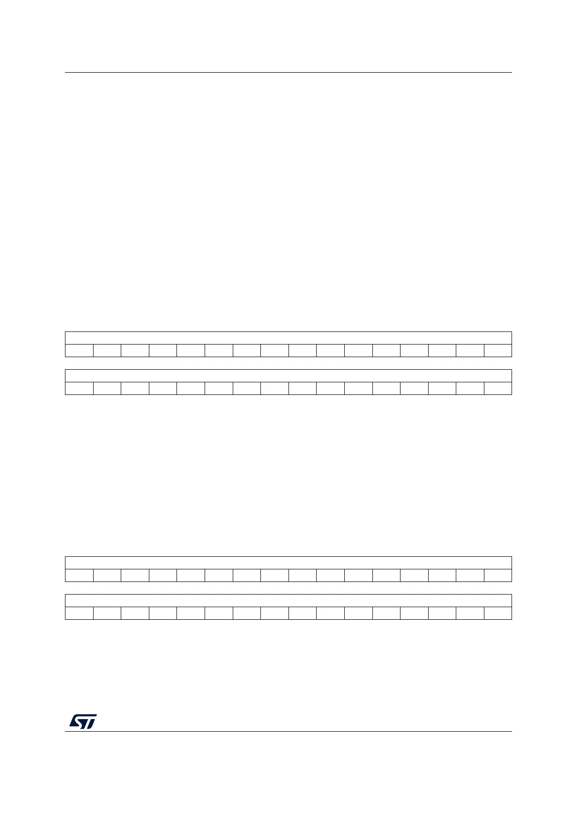
31 30 29 28 27 26 25 24 23 22 21 20 19 18 17 16
KEY[31:16]
wwwwwwwwwwwwwwww
1514131211109876543210
KEY[15:0]
wwwwwwwwwwwwwwww
Bits 31:0 KEY[31:0]: FLASH key
The following values must be written consecutively to unlock the FLASH control register
(FLASH_CR), thus enabling programming/erasing operations:
KEY1: 0x4567 0123
KEY2: 0xCDEF 89AB
31 30 29 28 27 26 25 24 23 22 21 20 19 18 17 16
OPTKEY[31:16]
wwwwwwwwwwwwwwww
1514131211109876543210
OPTKEY[15:0]
wwwwwwwwwwwwwwww
Bits 31:0 OPTKEY[31:0]: Option byte key
The following values must be written consecutively to unlock the Flash memory option
registers, enabling option byte programming/erasing operations:
KEY1: 0x0819 2A3B
KEY2: 0x4C5D 6E7F

 Loading...


