Embedded Flash memory (FLASH) RM0444
100/1390 RM0444 Rev 5
3.7 FLASH registers
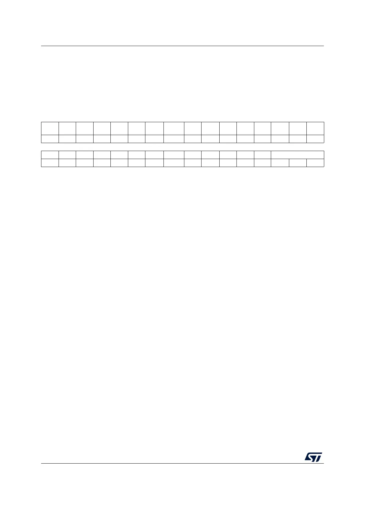
3.7.1 FLASH access control register (FLASH_ACR)
Address offset: 0x000
Reset value: 0x0004 0600
s
31 30 29 28 27 26 25 24 23 22 21 20 19 18 17 16
Res. Res. Res. Res. Res. Res. Res. Res. Res. Res. Res. Res. Res.
DBG
_SWEN
Res. EMPTY
rw rw
15 14 13 12 11 10 9 8 7 6 5 4 3 2 1 0
Res. Res. Res. Res. ICRST Res. ICEN PRFTEN Res. Res. Res. Res. Res. LATENCY[2:0]
rw rw rw rw rw rw
Bits 31:19 Reserved, must be kept at reset value.
Bit 18 DBG_SWEN: Debug access software enable
Software may use this bit to enable/disable the debugger read access.
0: Debugger disabled
1: Debugger enabled
Bit 17 Reserved, must be kept at reset value.
Bit 16 EMPTY: Main Flash memory area empty
This bit indicates whether the first location of the Main Flash memory area is erased or has a
programmed value.
0: Main Flash memory area programmed
1: Main Flash memory area empty
The bit can be set and reset by software..
Bits 15:12 Reserved, must be kept at reset value.
Bit 11 ICRST: CPU Instruction cache reset
0: CPU Instruction cache is not reset
1: CPU Instruction cache is reset
This bit can be written only when the instruction cache is disabled.
Bit 10 Reserved, must be kept at reset value.
Bit 9 ICEN: CPU Instruction cache enable
0: CPU Instruction cache is disabled
1: CPU Instruction cache is enabled

 Loading...


