RM0444 Rev 5 97/1390
RM0444 Embedded Flash memory (FLASH)
118
If an erase/program operation to a write-protected part of the Flash memory is attempted,
the write protection error flag (WRPERR) of the FLASH_SR register is set. This flag is also
set for any write access to:
–OTP area
– part of the Flash memory that can never be written like the ICP
– PCROP area
Note: When the Flash memory read protection level is selected (RDP level = 1), it is not possible
to program or erase the memory if the CPU debug features are connected (single wire) or
boot code is being executed from SRAM or system Flash memory, even if WRP is not
activated. Any attempt generates a hard fault (BusFault).
Note: To validate the WRP options, the option bytes must be reloaded by setting the
OBL_LAUNCH bit in Flash memory control register.
3.5.4 Securable memory area
The main purpose of the securable memory area is to protect a specific part of Flash
memory against undesired access. After system reset, the code in the securable memory
area can only be executed until the securable area becomes secured and never again until
the next system reset. This allows implementing software security services such as secure
key storage or safe boot.
Securable memory area is located in the Main Flash memory. It is dedicated to executing
trusted code. When not secured, the securable memory behaves like the rest of Main Flash
memory. When secured (the SEC_PROT and SEC_PROT2 bits of the FLASH_CR register
set, the latter pertaining to Bank 2 in dual-bank devices), any access to securable memory
area (fetch, read, programming, erase) is rejected, generating a bus error. The securable
area can only be unsecured by a system reset.
The size of the securable memory area is defined by the SEC_SIZE[7:0] and
SEC_SIZE2[7:0] (the latter for dual-bank devices only) bitfields of the FLASH_SECR
register. It can be modified only in RDP Level 0. Its content is erased upon changing from
RDP Level 1 to Level 0, even if it overlaps with PCROP subpages.
Note: The securable memory area start address is 0x0800 0000. Before activating the securable
memory area, move the vector table outside the page 0 if necessary.
Note: Upon change from RDP Level 1 to Level 0 while the PCROP_RDP bit is cleared, the
securable memory area is erased even if it overlaps with the PCROP subpages. The
PCROP subpages not overlapping with the securable memory area are not erased. See
Table 22.
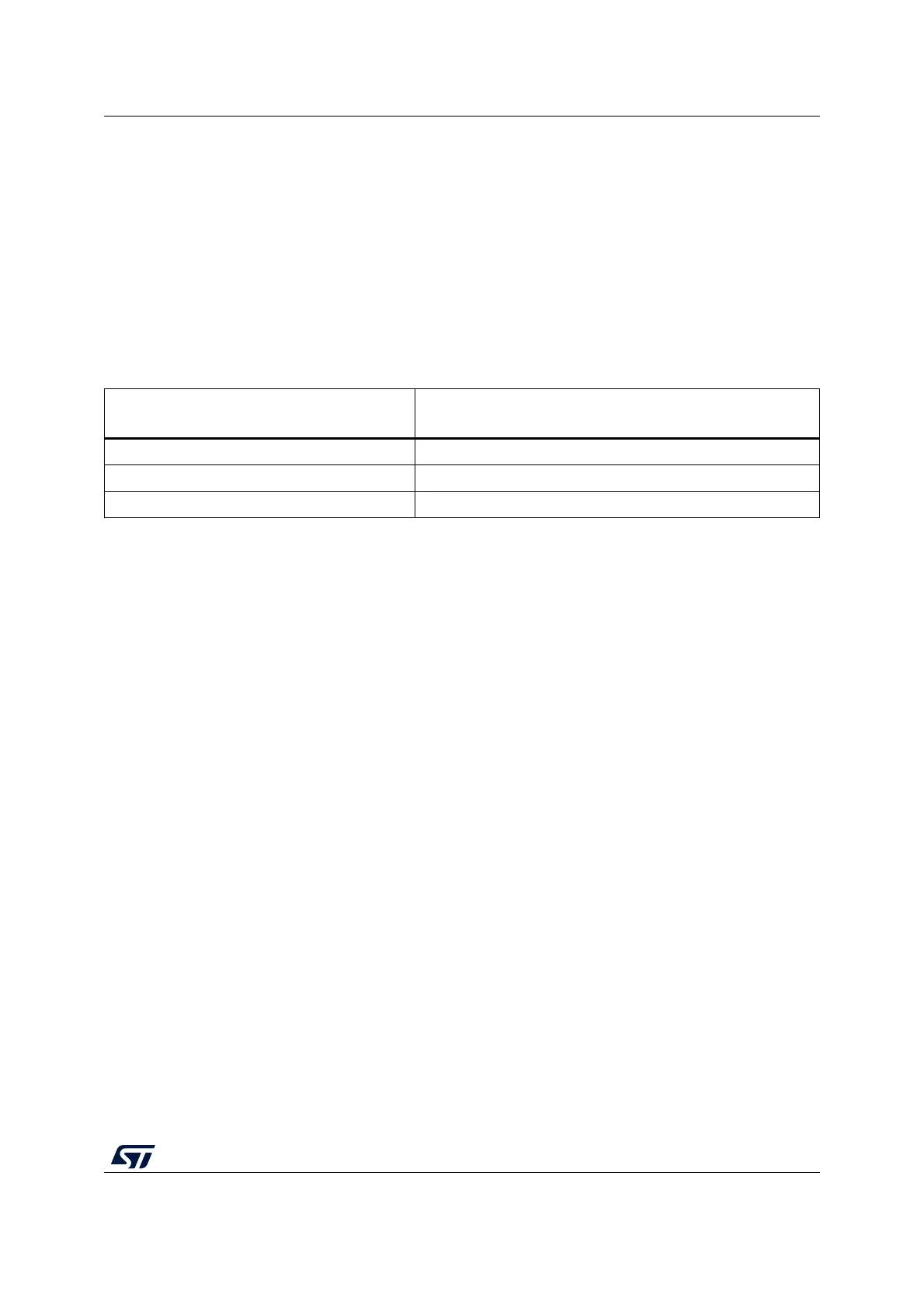
Table 21: WRP protection
WRP registers values
(x = A or B, y= 1 or 2)
WRP-protected area
WRPyx_STRT = WRPyx_END Page WRPyx
WRPyx_STRT > WRPyx_END None (unprotected)
WRPyx_STRT < WRPyx_END Pages from WRPyx_STRT to WRPyx_END

 Loading...


