Advanced-control timer (TIM1) RM0444
604/1390 RM0444 Rev 5
Note: The state of the external I/O pins connected to the complementary OCx and OCxN channels
depends on the OCx and OCxN channel state and the GPIO registers.
Bit 0 CC1E: Capture/Compare 1 output enable
0: Capture mode disabled / OC1 is not active (see below)
1: Capture mode enabled / OC1 signal is output on the corresponding output pin
When CC1 channel is configured as output, the OC1 level depends on MOE, OSSI,
OSSR, OIS1, OIS1N and CC1NE bits, regardless of the CC1E bits state. Refer to Table 116
for details.
Note: On channels having a complementary output, this bit is preloaded. If the CCPC bit is
set in the TIMx_CR2 register then the CC1E active bit takes the new value from the
preloaded bit only when a Commutation event is generated.
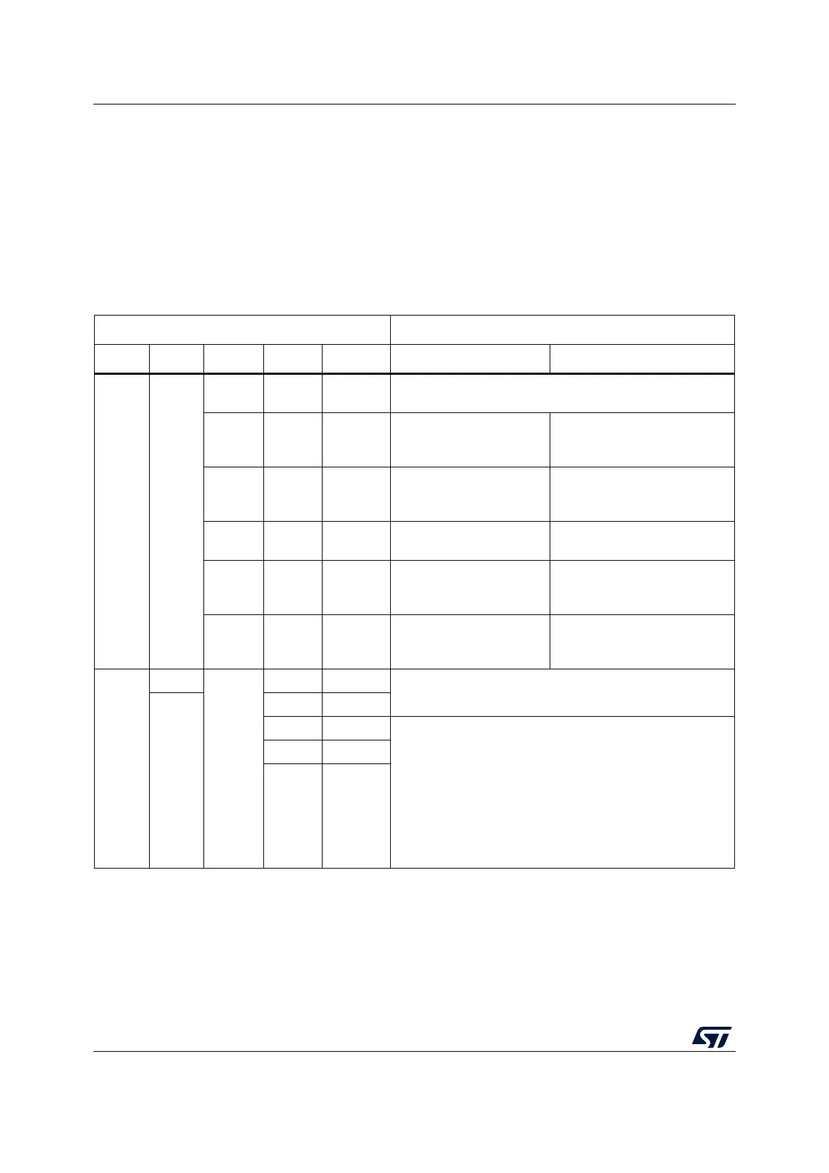
Table 116. Output control bits for complementary OCx and OCxN channels with break feature
Control bits Output states
(1)
MOE bit OSSI bit OSSR bit CCxE bit CCxNE bit OCx output state OCxN output state
1X
X0 0
Output disabled (not driven by the timer: Hi-Z)
OCx=0, OCxN=0
00 1
Output disabled (not driven
by the timer: Hi-Z)
OCx=0
OCxREF + Polarity
OCxN = OCxREF xor CCxNP
01 0
OCxREF + Polarity
OCx=OCxREF xor CCxP
Output Disabled (not driven by
the timer: Hi-Z)
OCxN=0
X1 1
OCREF + Polarity + dead-
time
Complementary to OCREF (not
OCREF) + Polarity + dead-time
10 1
Off-State (output enabled
with inactive state)
OCx=CCxP
OCxREF + Polarity
OCxN = OCxREF x or CCxNP
11 0
OCxREF + Polarity
OCx=OCxREF xor CCxP
Off-State (output enabled with
inactive state)
OCxN=CCxNP
0
0
X
XX
Output disabled (not driven by the timer: Hi-Z).
1
00
0 1 Off-State (output enabled with inactive state)
Asynchronously: OCx=CCxP, OCxN=CCxNP (if BRK or
BRK2 is triggered).
Then (this is valid only if BRK is triggered), if the clock is
present: OCx=OISx and OCxN=OISxN after a dead-time,
assuming that OISx and OISxN do not correspond to OCX
and OCxN both in active state (may cause a short circuit
when driving switches in half-bridge configuration).
Note: BRK2 can only be used if OSSI = OSSR = 1.
10
11
1. When both outputs of a channel are not used (control taken over by GPIO), the OISx, OISxN, CCxP and CCxNP bits must
be kept cleared.

 Loading...


