General-purpose timers (TIM15/TIM16/TIM17) RM0444
744/1390 RM0444 Rev 5
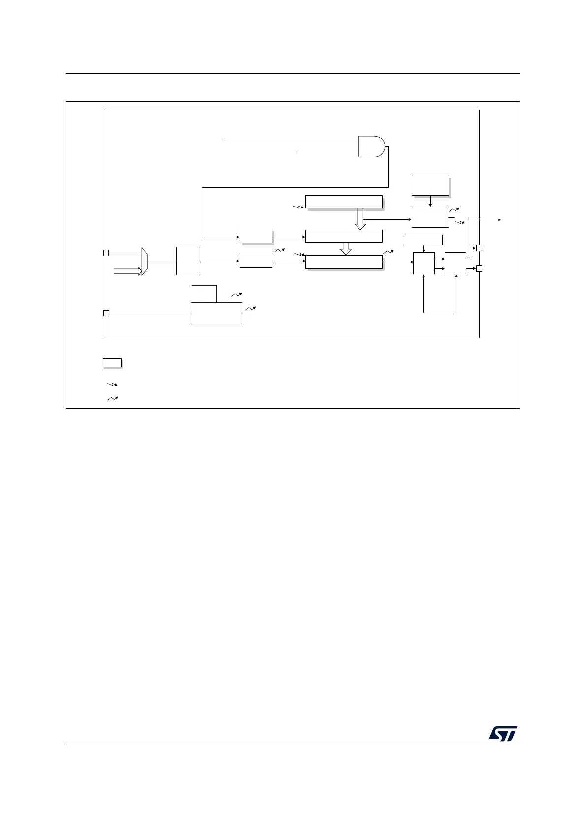
Figure 237. TIM16/TIM17 block diagram
1. This signal can be used as trigger for some slave timer, see Section 25.4.23: Using timer output as trigger for other timers
(TIM16/TIM17).
2. The internal break event source can be:
- A clock failure event generated by CSS. For further information on the CSS, refer to Section 5.2.9: Clock security system
(CSS)
- A PVD output
- SRAM parity error signal
- Cortex
®
-M0+ LOCKUP (Hardfault) output
- COMP output
MSv40937V2
Internal clock (CK_INT)
Counter Enable (CEN)
TIMx_CH1
TIMx_BKIN
Auto-reload register
CNT counter
+/-
Capture/compare 1 register
TI1FP1
IC1
REP register
Repetition
counter
DTG registers
DTG
Output
control
CK_PSC
CK_CNT
IC1PS
Stop, clear or up/down
OC1REF
CC1I
C1I
U
UI
U
OC1
OC1N
TIMx_CH1
TIMx_CH1N
Input
filter &
edge
detector
U
Notes:
Reg
Preload registers transferred
to active registers on U event
according to control bit
Event
Interrupt & DMA output
PSC
prescaler
Prescaler
Internal sources
SBIF
Break circuitry
(2)
BIF
BRK request
TI1[1..15]
TI1[0]
To other
timers for
cross-
trigerring
(1)

 Loading...


