RM0444 Rev 5 371/1390
RM0444 Analog-to-digital converter (ADC)
403
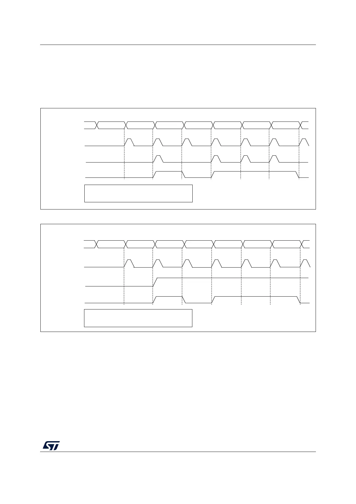
The AWD comparison is performed at the end of each ADC conversion. The
ADC_AWDx_OUT rising edge and falling edge occurs two ADC_CLK clock cycles after the
comparison.
As ADC_AWDx_OUT is generated by the ADC_CLK domain and AWD flag is generated by
the APB clock domain, the rising edges of these signals are not synchronized.
Figure 50. ADC_AWDx_OUT signal generation
Figure 51. ADC_AWDx_OUT signal generation (AWDx flag not cleared by software)
MSv45362V1
EOC FLAG
ADC STATE
RDY
AWDx FLAG
Conversion1
outside
ADC_AWDx_OUT
inside
Cleared
by SW
Conversion2 Conversion3 Conversion4 Conversion5 Conversion6 Conversion7
outsideinside outside outside inside
- Converted channels: 1,2,3,4,5,6,7
- Guarded converted channels: 1,2,3,4,5,6,7
Cleared
by SW
Cleared
by SW
Cleared
by SW
MSv45363V1
EOC FLAG
ADC STATE
RDY
AWDx FLAG
Conversion1
outside
ADC_AWDx_OUT
inside
not cleared by SW
Conversion2 Conversion3 Conversion4 Conversion5 Conversion6 Conversion7
outsideinside outside outside inside
- Converted channels: 1,2,3,4,5,6,7
- Guarded converted channels: 1,2,3,4,5,6,7

 Loading...


