RM0444 Rev 5 357/1390
RM0444 Analog-to-digital converter (ADC)
403
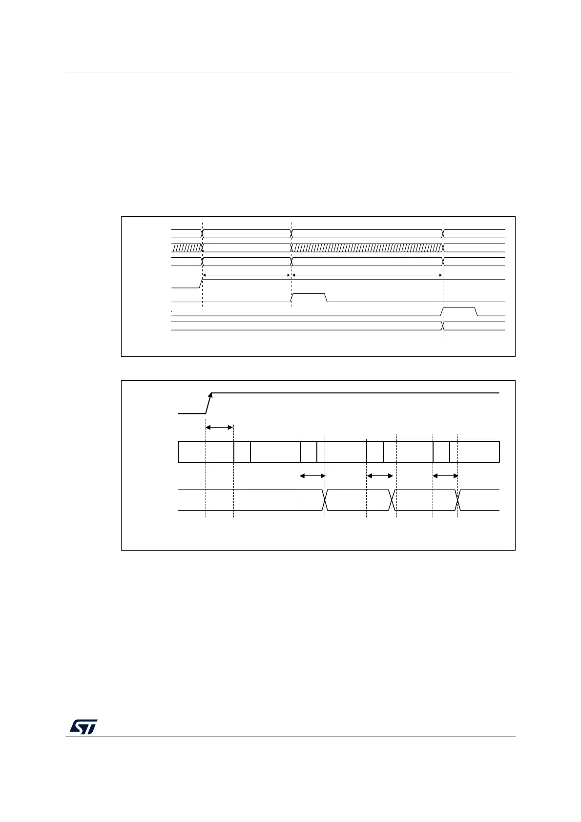
15.3.13 Timings
The elapsed time between the start of a conversion and the end of conversion is the sum of
the configured sampling time plus the successive approximation time depending on data
resolution:
Figure 37. Analog to digital conversion time
Figure 38. ADC conversion timings
1. EXTEN = 00 or EXTEN ≠ 00
2. Trigger latency (refer to datasheet for more details)
3. ADC_DR register write latency (refer to datasheet for more details)
t
CONV
= t
SMPL
+ t
SAR
= [1.5
|min
+ 12.5
|12bit
] x t
ADC_CLK
t
CONV
= t
SMPL
+ t
SAR
= 42.9 ns
|min
+ 357.1 ns
|12bit
= 0.400 µs
|min
(for f
ADC_CLK
= 35 MHz)
Analog
channel
Internal S/H
tt
depends on SMP[2:0]
set
by SW
EOSMP
cleared by SW
MS30336V1
DATA N-1
DATA N
CH(N)
CH(N+1)
ADC state
ADSTART
ADC_DR
EOC
SMPL
RDY
SAMPLING CH(N)
CONVERTING CH(N)
SAMPLING CH(N+1)
Sample AIN(N+1)
Hold AIN(N)
Sample AIN(N+1)
SAR
(1) (2)
set by HW
cleared
by SW
set
by HW
(1)
t
SMPL
depends on RES[2:0]
(2)
t
SAR
MSv33174V1
Ready S0 Conversion 0
t
LATENCY
(2)
ADSTART
(1)
ADC state
ADC_DR
S1 Conversion 1 S2 Conversion 2 S3 Conversion 3
W
LATENCY
(3)
W
LATENCY
(3)
W
LATENCY
(3)
Data 1Data 0 Data 2

 Loading...


