Digital-to-analog converter (DAC) RM0444
406/1390 RM0444 Rev 5
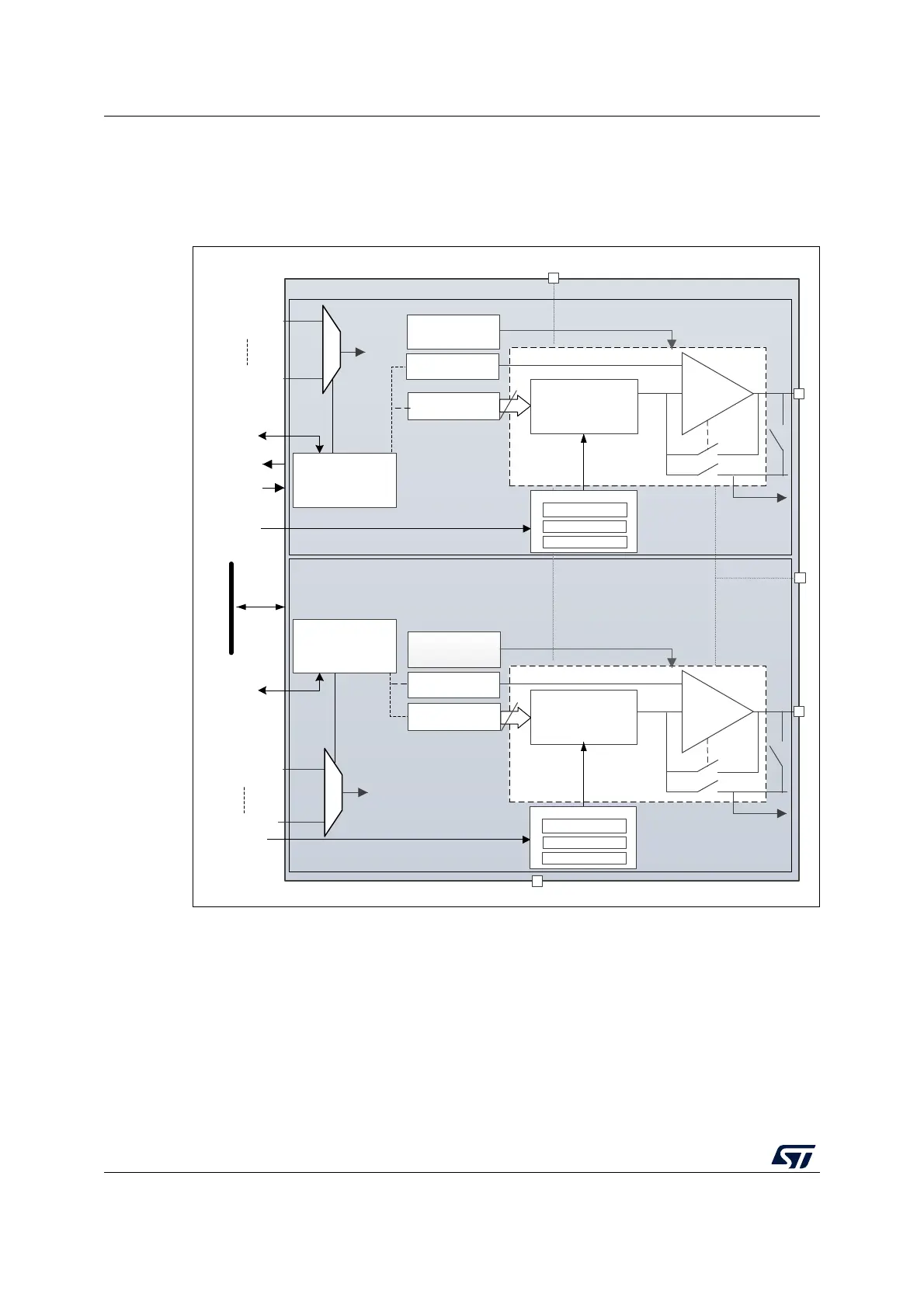
16.4 DAC functional description
16.4.1 DAC block diagram
Figure 59. Dual-channel DAC block diagram
1. MODEx bits in the DAC_MCR control the output mode and allow switching between the Normal mode in
buffer/unbuffered configuration and the Sample and hold mode.
2. Refer to Section 16.3: DAC implementation for channel2 availability.
MSv46119V5
VREF+
dac_out1
DAC_OUT1
Buffer
1
DAC_OUT2
Buffer
2
TSEL1
[3:0]
bits
dac_out2
TRIG
TSEL2
[3:0] bits
TRIG
Offset
calibration
dac_ch1_dma
dac_ch1_trg1
dac_ch1_trg15
dac_ch2_trg1
dac_ch2_trg15
OTRIM2[5:0]
bits
32-bit APB
bus
Control registers
& logic Channel2
dac_ch2_dma
DOR1
Offset
calibration
OTRIM1[5:0]
bits
DAC
converter 2
12-bit
12-bit
MODE1 bits
MODE2 bits
dac_unr_it
dac_pclk
DOR2
VDD
VSS
DAC channel 1
DAC channel 2
dac_hold
_ck
Control registers
& logic Channel1
dac_hold
_ck
DAC
converter 1
Sample & Hold registers
TSAMPLE2
TREFRESH2
THOLD2
Sample & Hold registers
TSAMPLE1
TREFRESH1
THOLD1

 Loading...


