RM0444 Rev 5 345/1390
RM0444 Analog-to-digital converter (ADC)
403
15.3 ADC functional description
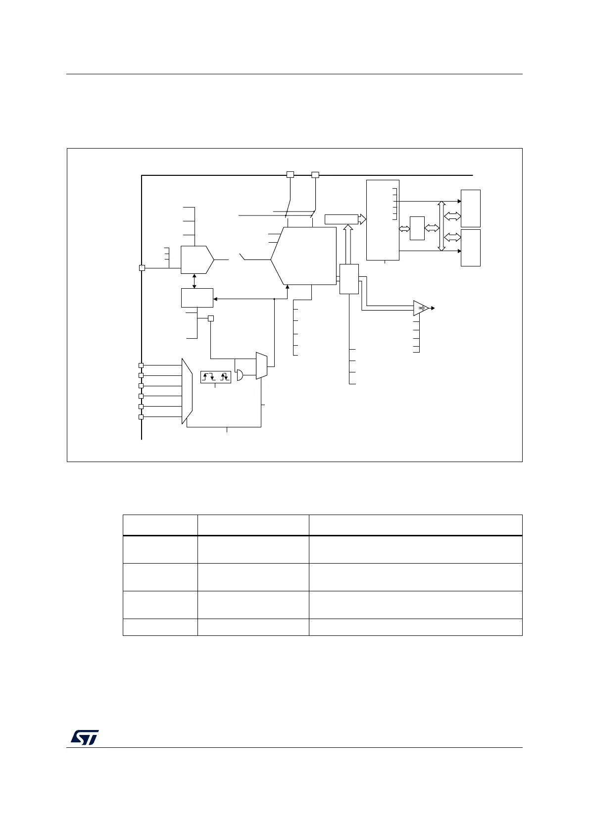
Figure 31 shows the ADC block diagram and Table 68 gives the ADC pin description.
Figure 31. ADC block diagram
15.3.1 ADC pins and internal signals
MSv47996V3
DATA[15:0]
AHB
to
APB
APB
interface
DMA
CPU
Start & stop
control
TIM1_TRGO2
ADC_IN
[18:15, 11:0]
SAR ADC
V
IN
Supply &
reference
VREF+
TIM2_TRGO
TIM6_TRGO
TIM1_CC4
Input
selection
& scan
control
SMP[2:0]
sampling
time
start
ADCAL self
calibration
LFTRIG
CONVERTED
DATA
SCANDIR
up/down
CH_SEL[18:0]
CONT
single/cont.
ADEN/ADDIS
VDD/VDDA
AUTOFF
Auto-off mode
AREADY
EOSMP
EOSEQ
EOC
OVR
AWD
ADC interrupt
IRQ
DMA request
AHB
DMAEN
DMACFG
OVRMODE
(overrun mode)
ALIGN (left/right)
RES[1:0]
(12, 10, 8 bits)
JOFFSETx[11:0]
JOFFSETx_
CH[11:0]
AWDxEN
AWDxSGL
AWDCHx[4:0]
LTx[11:0]
HTx[11:0]
ADC_AWDx_OUT
To analog watchdog
ADSTART
SW trigger
AUTDLY
Auto-delayed
conversion
ADSTP
stop conversion
EXTEND[1:0]
Trigger enable
and edge
selection
EXTSEL[1:0]
Trigger selection
DISCEN
Discontinuous
mode
HW
trigger
slave
Master
Master
Oversa
mpler
TOVS
OVSS[3:0]
OVSR[3:0]
OVSE
TIM3_TRGO
TIM15_TRGO
V
IN[x]
V
BAT
V
REFINT
V
SENSE
Table 68. ADC input/output pins
Name Signal type Remarks
VDDA
Input, analog power
supply
Analog power supply and positive reference voltage
for the ADC, V
DDA
≥ V
DD
VSSA
Input, analog supply
ground
Ground for analog power supply. Must be at V
SS
potential
VREF+
Input, analog reference
positive
The higher/positive reference voltage for the ADC.
ADC_INx Analog input signals 16 external analog input channels

 Loading...


