Advanced-control timer (TIM1) RM0444
608/1390 RM0444 Rev 5
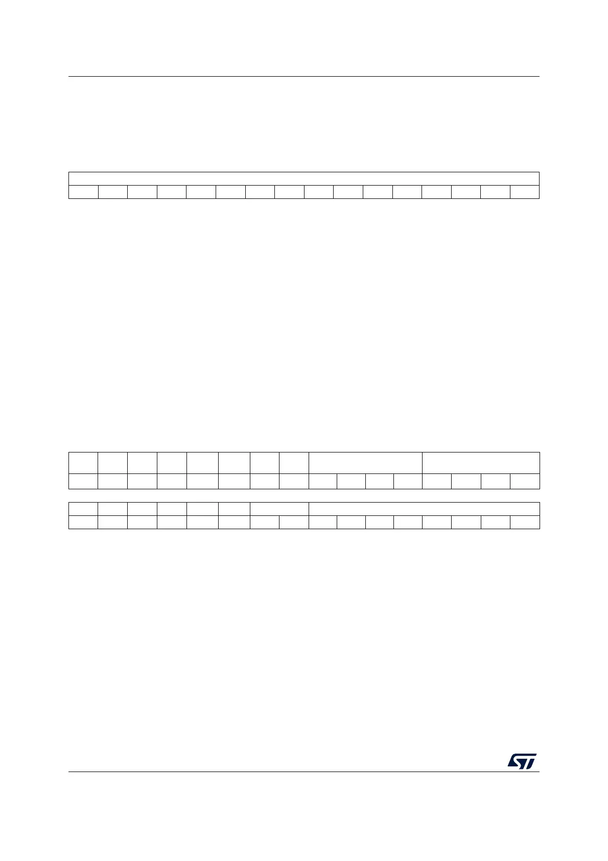
21.4.19 TIM1 capture/compare register 4 (TIM1_CCR4)
Address offset: 0x40
Reset value: 0x0000
21.4.20 TIM1 break and dead-time register
(TIM1_BDTR)
Address offset: 0x44
Reset value: 0x0000 0000
Note: As the bits BK2BID, BKBID, BK2DSRM, BKDSRM, BK2P, BK2E, BK2F[3:0], BKF[3:0],
AOE, BKP, BKE, OSSI, OSSR and DTG[7:0] can be write-locked depending on the LOCK
configuration, it can be necessary to configure all of them during the first write access to the
TIMx_BDTR register.
1514131211109876543210
CCR4[15:0]
rw rw rw rw rw rw rw rw rw rw rw rw rw rw rw rw
Bits 15:0 CCR4[15:0]: Capture/Compare value
If channel CC4 is configured as output: CCR4 is the value to be loaded in the actual
capture/compare 4 register (preload value).
It is loaded permanently if the preload feature is not selected in the TIMx_CCMR2 register
(bit OC4PE). Else the preload value is copied in the active capture/compare 4 register when
an update event occurs.
The active capture/compare register contains the value to be compared to the counter
TIMx_CNT and signalled on OC4 output.
If channel CC4 is configured as input: CCR4 is the counter value transferred by the last
input capture 4 event (IC4). The TIMx_CCR4 register is read-only and cannot be
programmed.
31 30 29 28 27 26 25 24 23 22 21 20 19 18 17 16
Res. Res. BK2BID BKBID
BK2
DSRM
BK
DSRM
BK2P BK2E BK2F[3:0] BKF[3:0]
rw rw rw rw rw rw rw rw rw rw rw rw rw rw
1514131211109876543210
MOE AOE BKP BKE OSSR OSSI LOCK[1:0] DTG[7:0]
rw rw rw rw rw rw rw rw rw rw rw rw rw rw rw rw
Bits 31:30 Reserved, must be kept at reset value.
Bit 29 BK2BID: Break2 bidirectional
Refer to BKBID description

 Loading...


