General-purpose timers (TIM2/TIM3/TIM4) RM0444
668/1390 RM0444 Rev 5
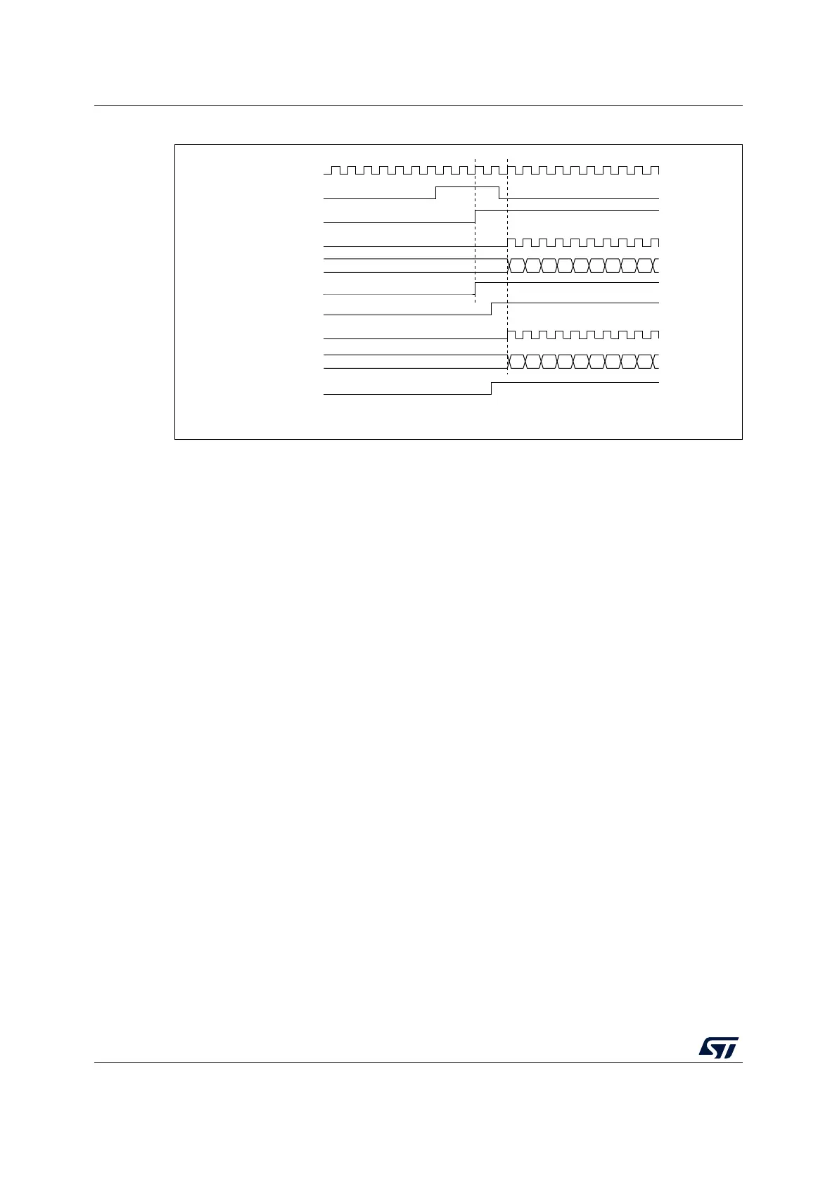
Figure 210. Triggering TIM3 and TIM2 with TIM3 TI1 input
Note: The clock of the slave peripherals (timer, ADC, ...) receiving the TRGO or the TRGO2
signals must be enabled prior to receive events from the master timer, and the clock
frequency (prescaler) must not be changed on-the-fly while triggers are received from the
master timer.
22.3.20 DMA burst mode
The TIMx timers have the capability to generate multiple DMA requests upon a single event.
The main purpose is to be able to re-program part of the timer multiple times without
software overhead, but it can also be used to read several registers in a row, at regular
intervals.
The DMA controller destination is unique and must point to the virtual register TIMx_DMAR.
On a given timer event, the timer launches a sequence of DMA requests (burst). Each write
into the TIMx_DMAR register is actually redirected to one of the timer registers.
The DBL[4:0] bits in the TIMx_DCR register set the DMA burst length. The timer recognizes
a burst transfer when a read or a write access is done to the TIMx_DMAR address), i.e. the
number of transfers (either in half-words or in bytes).
The DBA[4:0] bits in the TIMx_DCR registers define the DMA base address for DMA
transfers (when read/write access are done through the TIMx_DMAR address). DBA is
defined as an offset starting from the address of the TIMx_CR1 register:
Example:
00000: TIMx_CR1
00001: TIMx_CR2
00010: TIMx_SMCR
As an example, the timer DMA burst feature is used to update the contents of the CCRx
registers (x = 2, 3, 4) upon an update event, with the DMA transferring half words into the
CCRx registers.
This is done in the following steps:
MS33123V1
CK_INT
TIM2-CNT
TIM3-CEN=CNT_EN
TIM2-TIF
01
TIM3-CNT
02 03 04 05 06 07 08 09
00
01 02 03 04 05 06 07 08 0900
TIM2-CEN=CNT_EN
TIM3-TIF
TIM3-CK_PSC
TIM3-TI1
TIM2-CK_PSC

 Loading...


