Embedded Flash memory (FLASH) RM0444
108/1390 RM0444 Rev 5
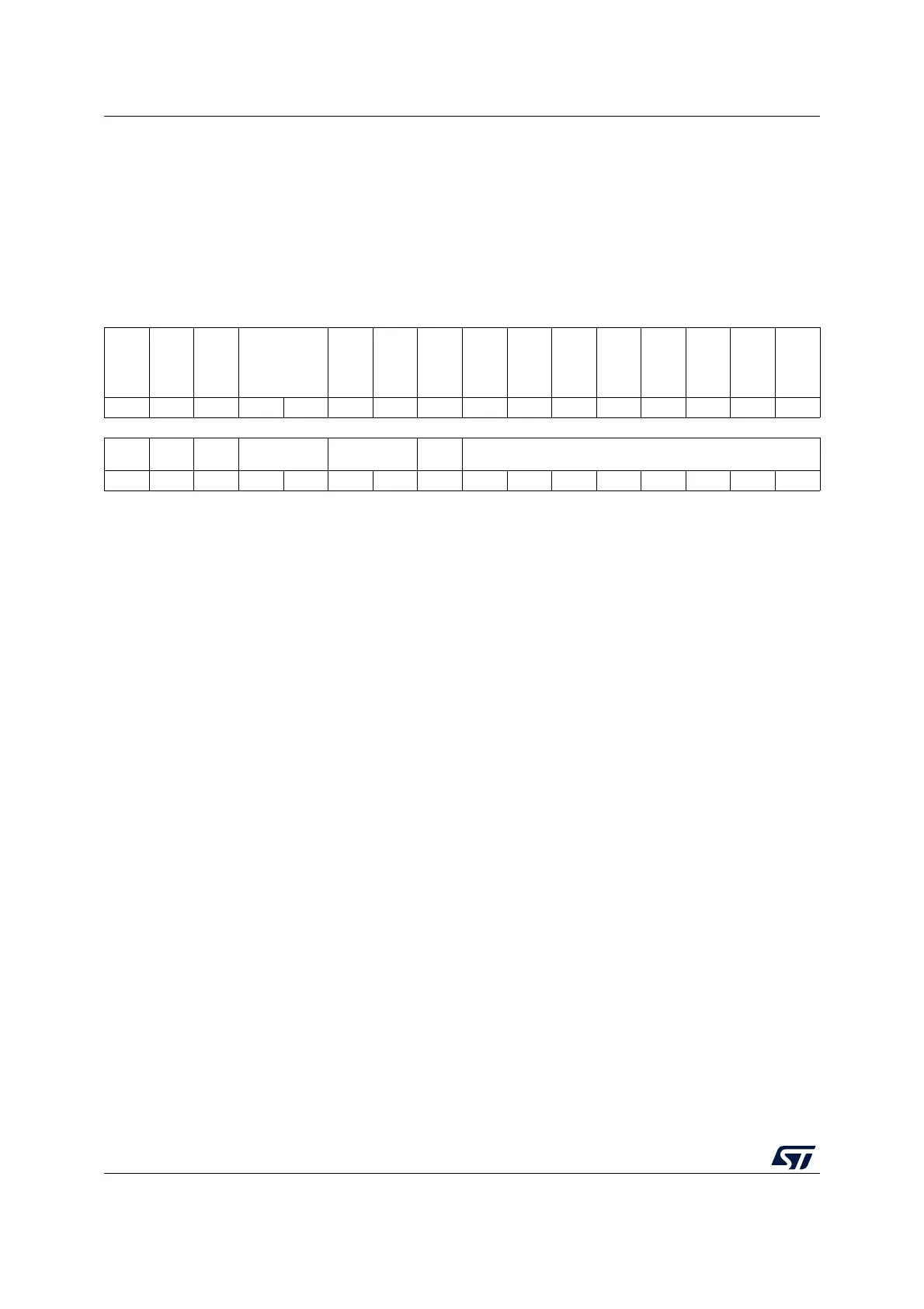
3.7.8 FLASH option register (FLASH_OPTR)
Address offset: 0x020
Reset value: 0b11XX XXXX 1X1X XXXX XXXX XXXX XXXX XXXX (The option bits are
loaded with values from Flash memory at power-on reset release.)
Access: no wait state when no Flash memory operation is on going, word, half-word and
byte access
31 30 29 28 27 26 25 24 23 22 21 20 19 18 17 16
Res. Res. IRHEN
NRST_MODE
[1:0]
n
BOOT0
n
BOOT1
nBOOT
_SEL
Res.
RAM
_
PARITY
_
CHECK
DUAL_
BANK
SWAP
_BANK
WWDG
_SW
IWGD
_
STDBY
IWDG
_STOP
IWDG
_SW
rw rw rw rw rw rw rw rw rw rw rw rw rw
1514131211109876543210
nRST_
SHDW
nRST_
STDBY
nRST_
STOP
BORF_LEV[1:0] BORR_LEV[1:0]
BOR_
EN
RDP[7:0]
rw rw rw rw rw rw rw rw rw rw rw rw rw rw rw rw
Bits 31:30 Reserved, must be kept at reset value.
Bit 29 IRHEN: Internal reset holder enable bit
0: Internal resets are propagated as simple pulse on NRST pin
1: Internal resets drives NRST pin low until it is seen as low level
Bits 28:27 NRST_MODE[1:0]
00: Reserved
01: Reset Input only: a low level on the NRST pin generates system reset, internal RESET
not propagated to the NSRT pin
10: GPIO: standard GPIO pad functionality, only internal RESET possible
11: Bidirectional reset: NRST pin configured in reset input/output mode (legacy mode)
Bit 26 nBOOT0: nBOOT0 option bit
0: nBOOT0=0
1: nBOOT0=1
Bit 25 nBOOT1: Boot configuration
Together with the BOOT0 pin or option bit nBOOT0 (depending on nBOOT_SEL option bit
configuration), this bit selects boot mode from the Main Flash memory, SRAM or the
System memory. Refer to Section 2.5: Boot configuration
Bit 24 nBOOT_SEL
0: BOOT0 signal is defined by BOOT0 pin value (legacy mode)
1: BOOT0 signal is defined by nBOOT0 option bit
Bit 23 Reserved, must be kept at reset value.
Bit 22 RAM_PARITY_CHECK: SRAM parity check control
0: SRAM parity check enable
1: SRAM parity check disable
Bit 21 DUAL_BANK: Dual-bank on 512 Kbytes or 256 Kbytes Flash memory devices
0: 256 Kbytes/512 Kbytes single-bank Flash memory, contiguous addresses in Bank 1
1: 256 Kbytes/512 Kbytes dual-bank Flash memory, Refer to Table 10 and Table 11

 Loading...


