RM0444 Rev 5 803/1390
RM0444 General-purpose timers (TIM15/TIM16/TIM17)
830
25.5.20 TIM15 input selection register (TIM15_TISEL)
Address offset: 0x68
Reset value: 0x0000 0000
Bits 8:4 Reserved, must be kept at reset value.
Bit 3 BKCMP3E: BRK COMP3 enable
This bit enables the COMP3 for the timer’s BRK input. COMP3 output is ‘ORed’ with the
other BRK sources.
0: COMP3 input disabled
1: COMP3 input enabled
Note: This bit can not be modified as long as LOCK level 1 has been programmed (LOCK bits
in TIMx_BDTR register).
Bit 2 BKCMP2E: BRK COMP2 enable
This bit enables the COMP2 for the timer’s BRK input. COMP2 output is ‘ORed’ with the
other BRK sources.
0: COMP2 input disabled
1: COMP2 input enabled
Note: This bit can not be modified as long as LOCK level 1 has been programmed (LOCK bits
in TIMx_BDTR register).
Bit 1 BKCMP1E: BRK COMP1 enable
This bit enables the COMP1 for the timer’s BRK input. COMP1 output is ‘ORed’ with the
other BRK sources.
0: COMP1 input disabled
1: COMP1 input enabled
Note: This bit can not be modified as long as LOCK level 1 has been programmed (LOCK bits
in TIMx_BDTR register).
Bit 0 BKINE: BRK BKIN input enable
This bit enables the BKIN alternate function input for the timer’s BRK input. BKIN input is
‘ORed’ with the other BRK sources.
0: BKIN input disabled
1: BKIN input enabled
Note: This bit can not be modified as long as LOCK level 1 has been programmed (LOCK bits
in TIMx_BDTR register).
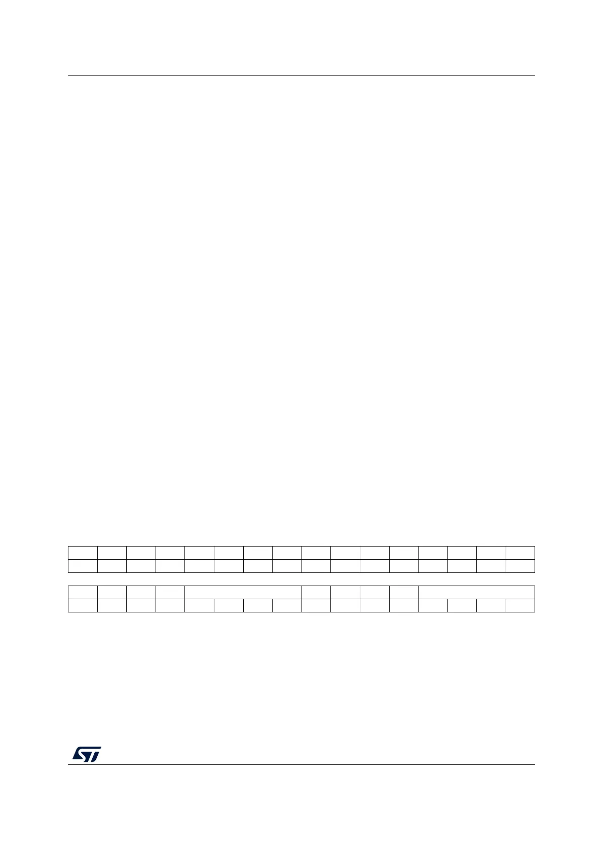
31 30 29 28 27 26 25 24 23 22 21 20 19 18 17 16
Res. Res. Res. Res. Res. Res. Res. Res. Res. Res. Res. Res. Res. Res. Res. Res.
1514131211109876543210
Res. Res. Res. Res. TI2SEL[3:0] Res. Res. Res. Res. TI1SEL[3:0]
rw rw rw rw rw rw rw rw
Bits 31:12 Reserved, must be kept at reset value.
Bits 11:8 TI2SEL[3:0]: selects TI2[0] to TI2[15] input
0000: TIM15_CH2 input
0001: TIM2_IC2
0010: TIM3_IC2
Others: Reserved
Bits 7:4 Reserved, must be kept at reset value.

 Loading...


