RM0444 Rev 5 81/1390
RM0444 Embedded Flash memory (FLASH)
118
User and read protection option bytes
Flash memory address: 0x1FFF 7800
Reset value: 0xFFFF FEAA (ST production value)
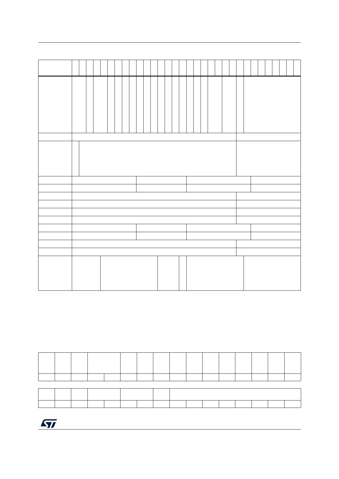
Table 16. Organization of option bytes
Address
(1)
31
30
29
28
27
26
25
24
23
22
21
20
19
18
17
16
15
14
13
12
11
10
9
8
7
6
5
4
3
2
1
0
0x1FFF7800
Reserved
IRHEN
NRST_MODE
nBOOT0
nBOOT1
nBOOT_SEL
Reserved
RAM_PARITY_CHECK
DUAL_BANK
nSWAP_BANK
WWDG_SW
IWDG_STBY
IWDG_STOP
IWDG_SW
nRST_SHDW
nRST_STDBY
nRST_STOP
BORF_LEV
BORR_LEV
BOR_EN
RDP
0x1FFF7808 Reserved PCROP1A_STRT
0x1FFF7810
PCROP_RDP
Reserved PCROP1A_END
0x1FFF7818 Reserved WRP1A_END Reserved WRP1A_STRT
0x1FFF7820 Reserved WRP1B_END Reserved WRP1B_STRT
0x1FFF7828 Reserved PCROP1B_STRT
0x1FFF7830 Reserved PCROP1B_END
0x1FFF7838 Reserved PCROP2A_STRT
0x1FFF7840 Reserved PCROP2A_END
0x1FFF7848 Reserved WRP2A_END Reserved WRP2A_STRT
0x1FFF7850 Reserved WRP2B_END Reserved WRP2B_STRT
0x1FFF7858 Reserved PCROP2B_STRT
0x1FFF7860 Reserved PCROP2B_END
0x1FFF7870 Reserved SEC_SIZE2 Res.
BOOT_LOCK
Reserved SEC_SIZE
1. The upper 32-bits of the double-word address contain the inverted data from the lower 32 bits.
31 30 29 28 27 26 25 24 23 22 21 20 19 18 17 16
Res. Res. IRHEN
NRST_MODE
[1:0]
n
BOOT0
n
BOOT1
nBOOT
_SEL
Res.
RAM_
PARITY
_
CHECK
DUAL_
BANK
nSWAP
_BANK
WWDG
_SW
IWGD
_STDB
Y
IWDG
_STOP
IWDG
_SW
rrrrrr rrrrrrr
1514131211109876543210
nRST_
SHDW
nRST_
STDBY
nRST_
STOP
BORF_LEV[1:0] BORR_LEV[1:0]
BOR_
EN
RDP[7:0]
rrrrrrrrrrrrrrrr

 Loading...


