Low-power timer (LPTIM) RM0444
832/1390 RM0444 Rev 5
26.3 LPTIM implementation
Table 131 describes LPTIM implementation on STM32G0x1 devices: the full set of features
is implemented in LPTIM1. LPTIM2 supports a smaller set of features, but is otherwise
identical to LPTIM1.
26.4 LPTIM functional description
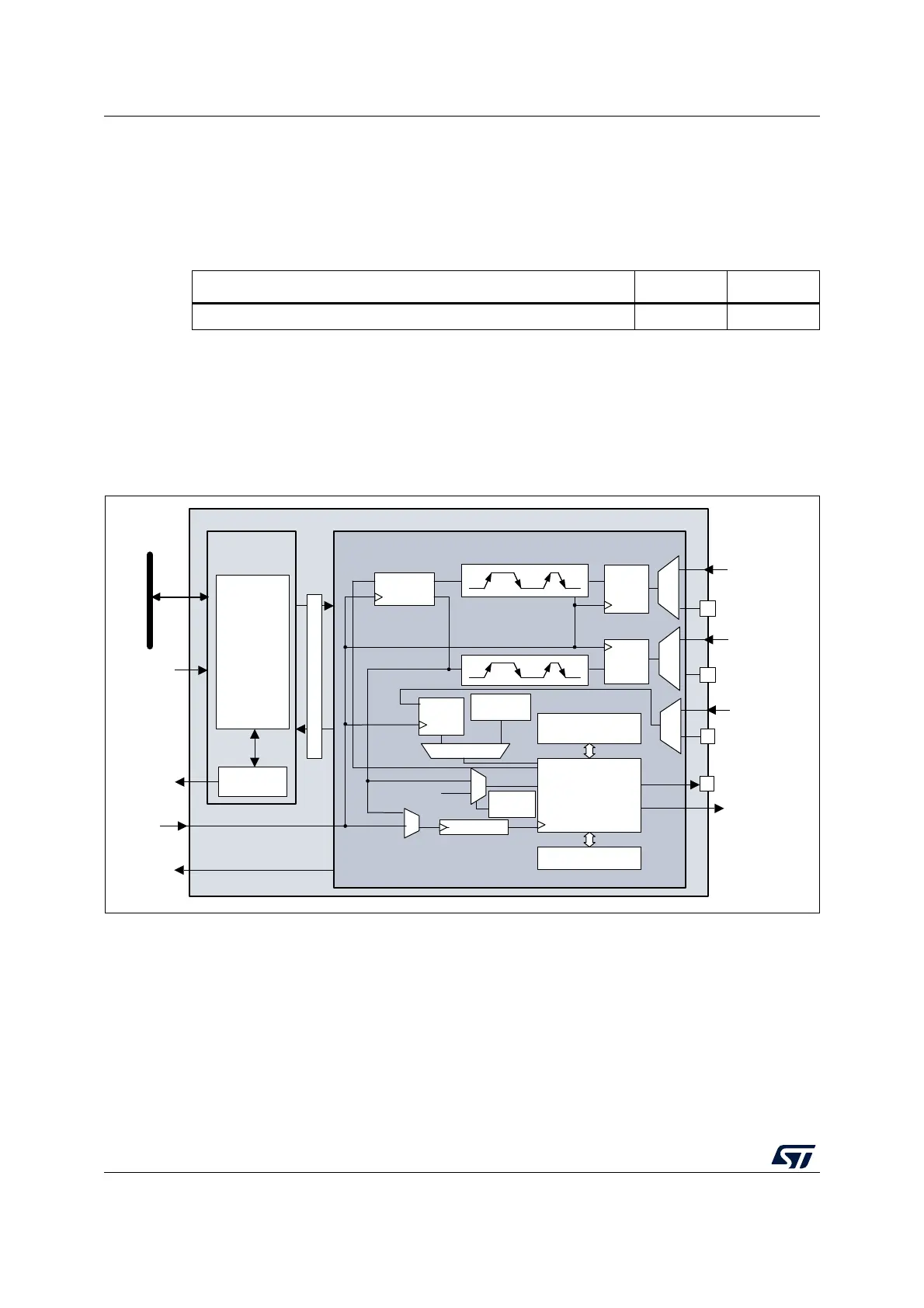
26.4.1 LPTIM block diagram
Figure 270. Low-power timer block diagram (LPTIM1 and LPTIM2
(1)
)
1. LPTIM2 has only the input channel 1, no input channel 2
2. lptim_out is the internal LPTIM output signal that can be connected to internal peripherals.
Table 131. STM32G0x1 LPTIM features
LPTIM modes/features
(1)
1. X = supported.
LPTIM1 LPTIM2
Encoder mode X -
MSv47463V1
LPTIM
lptim_ker_ck clock domain
CLKMUX
16-bit counter
16-bit ARR
LPTIM_OUT
Prescaler
Mux trigger
Glitch
filter
Glitch
filter
LPTIM_IN1
Encoder
Glitch
filter
Up/down
1
1
0
1
0
Count
mode
lptim_ext_trigx
LPTIM_IN2
lptim_in2_mux1
lptim_in2_mux2
lptim_in2_mux3
lptim_
ker_ck
lptim_it
IRQ
interface
LPTIM
register
interface
lptim_pclk
Synchronzation
CNTSTRT/
SNGSTRT
lptim_pclk
clock domain
32-bit APB bus
lptim_in1_mux1
lptim_in1_mux2
lptim_in1_mux3
LPTIM_ETR
lptim_out
(2)
lptim_
wkup
16-bit compare

 Loading...


