Reset and clock control (RCC) RM0444
186/1390 RM0444 Rev 5
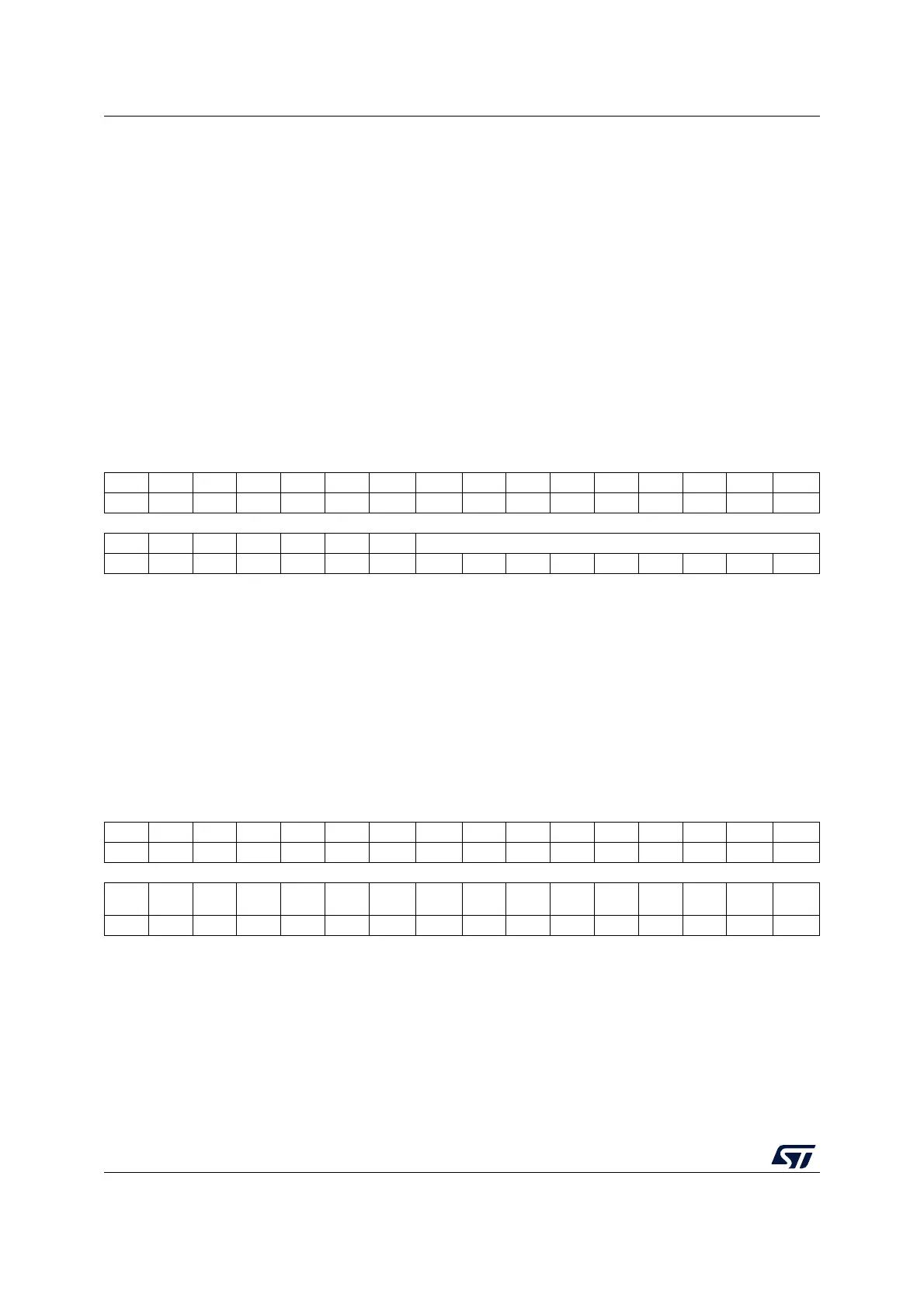
5.4.5 RCC clock recovery RC register (RCC_CRRCR)
This register applies to STM32G0B1xx and STM32G0C1xx only. It is reserved otherwise.
Address offset: 0x14
Reset value: 0x0000 0000 0000 0000 0000 000x xxxx xxxx
5.4.6 Clock interrupt enable register (RCC_CIER)
Address offset: 0x18
Reset value: 0x0000 0000
Bits 1:0 PLLSRC: PLL input clock source
This bit is controlled by software to select PLL clock source, as follows:
00: No clock
01: Reserved
10: HSI16
11: HSE
The bitfield can be written only when the PLL is disabled.
When the PLL is not used, selecting 00 allows saving power.
31 30 29 28 27 26 25 24 23 22 21 20 19 18 17 16
Res. Res. Res. Res. Res. Res. Res. Res. Res. Res. Res. Res. Res. Res. Res. Res.
1514131211109 8 765432 1 0
Res. Res. Res. Res. Res. Res. Res. HSI48CAL[8:0]
r rrrrrrr r
Bits 31:9 Reserved, must be kept at reset value.
Bits 8:0 HSI48CAL[8:0]: HSI48 clock calibration
These bits are initialized at startup with the factory-programmed HSI48 calibration trim
value.
31 30 29 28 27 26 25 24 23 22 21 20 19 18 17 16
Res. Res. Res. Res. Res. Res. Res. Res. Res. Res. Res. Res. Res. Res. Res. Res.
1514131211109 8 765432 1 0
Res. Res. Res. Res. Res. Res. Res. Res. Res. Res.
PLL
RDYIE
HSE
RDYIE
HSI
RDYIE
HSI48
RDYIE
LSE
RDYIE
LSI
RDYIE
rw rw rw rw rw rw

 Loading...


