RM0444 Rev 5 437/1390
RM0444 Digital-to-analog converter (DAC)
441
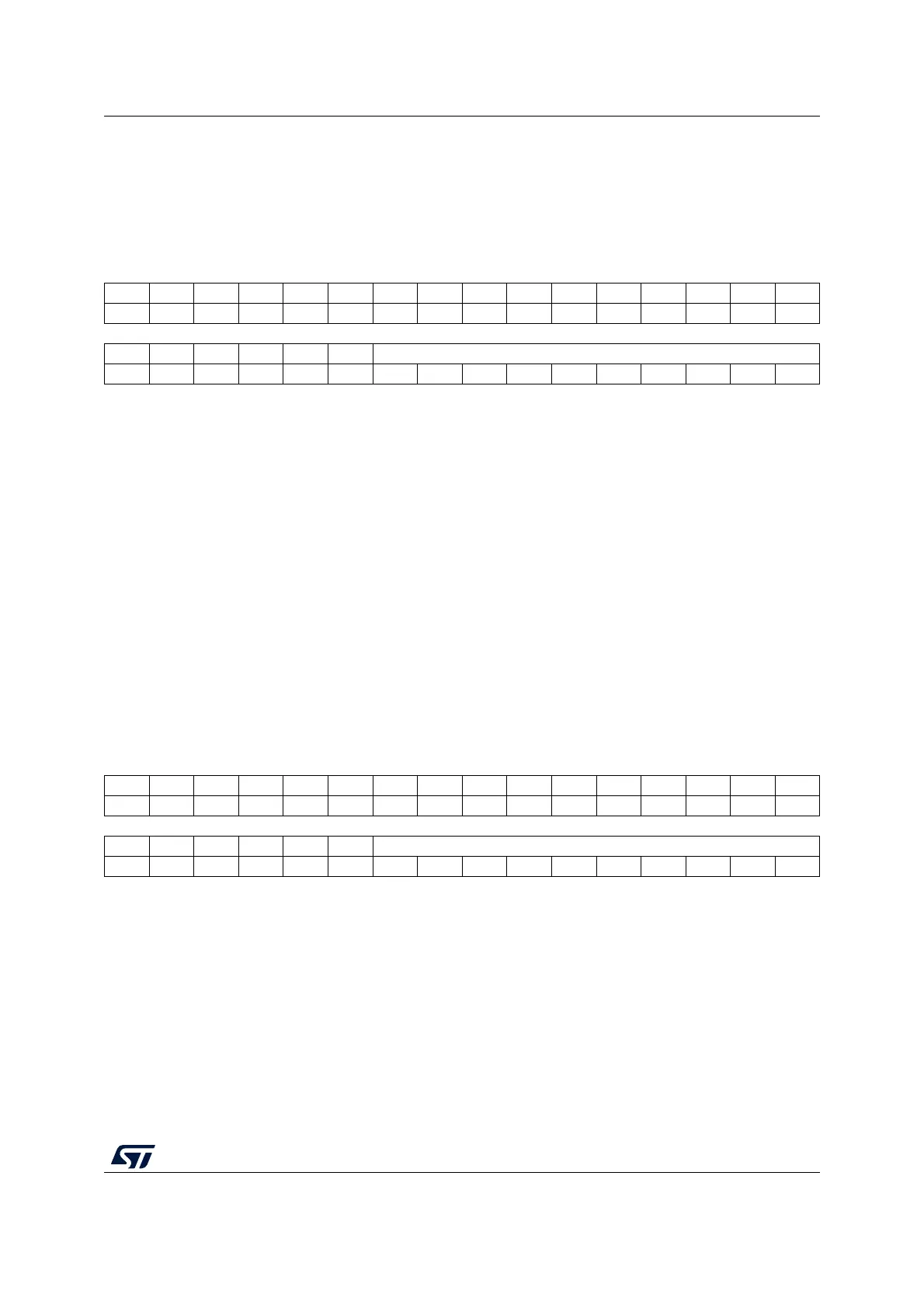
16.7.17 DAC channel1 sample and hold sample time register
(DAC_SHSR1)
Address offset: 0x40
Reset value: 0x0000 0000
Note: It represents the number of LSI clocks to perform a sample phase. Sampling time =
(TSAMPLE1[9:0] + 1) x LSI clock period.
16.7.18 DAC channel2 sample and hold sample time register
(DAC_SHSR2)
This register is available only on dual-channel DACs. Refer to Section 16.3: DAC
implementation.
Address offset: 0x44
Reset value: 0x0000 0000
Note: It represents the number of LSI clocks to perform a sample phase. Sampling time =
(TSAMPLE1[9:0] + 1) x LSI clock period.
31 30 29 28 27 26 25 24 23 22 21 20 19 18 17 16
Res. Res. Res. Res. Res. Res. Res. Res. Res. Res. Res. Res. Res. Res. Res. Res.
1514131211109876543210
Res. Res. Res. Res. Res. Res. TSAMPLE1[9:0]
rw rw rw rw rw rw rw rw rw rw
Bits 31:10 Reserved, must be kept at reset value.
Bits 9:0 TSAMPLE1[9:0]: DAC channel1 sample time (only valid in Sample and hold mode)
These bits can be written when the DAC channel1 is disabled or also during normal operation.
in the latter case, the write can be done only when BWST1 of DAC_SR register is low, If
BWST1=1, the write operation is ignored.
31 30 29 28 27 26 25 24 23 22 21 20 19 18 17 16
Res. Res. Res. Res. Res. Res. Res. Res. Res. Res. Res. Res. Res. Res. Res. Res.
1514131211109876543210
Res. Res. Res. Res. Res. Res. TSAMPLE2[9:0]
rw rw rw rw rw rw rw rw rw rw
Bits 31:10 Reserved, must be kept at reset value.
Bits 9:0 TSAMPLE2[9:0]: DAC channel2 sample time (only valid in Sample and hold mode)
These bits can be written when the DAC channel2 is disabled or also during normal
operation. in the latter case, the write can be done only when BWST2 of DAC_SR register is
low, if BWST2=1, the write operation is ignored.

 Loading...


