Advanced-control timer (TIM1) RM0444
614/1390 RM0444 Rev 5
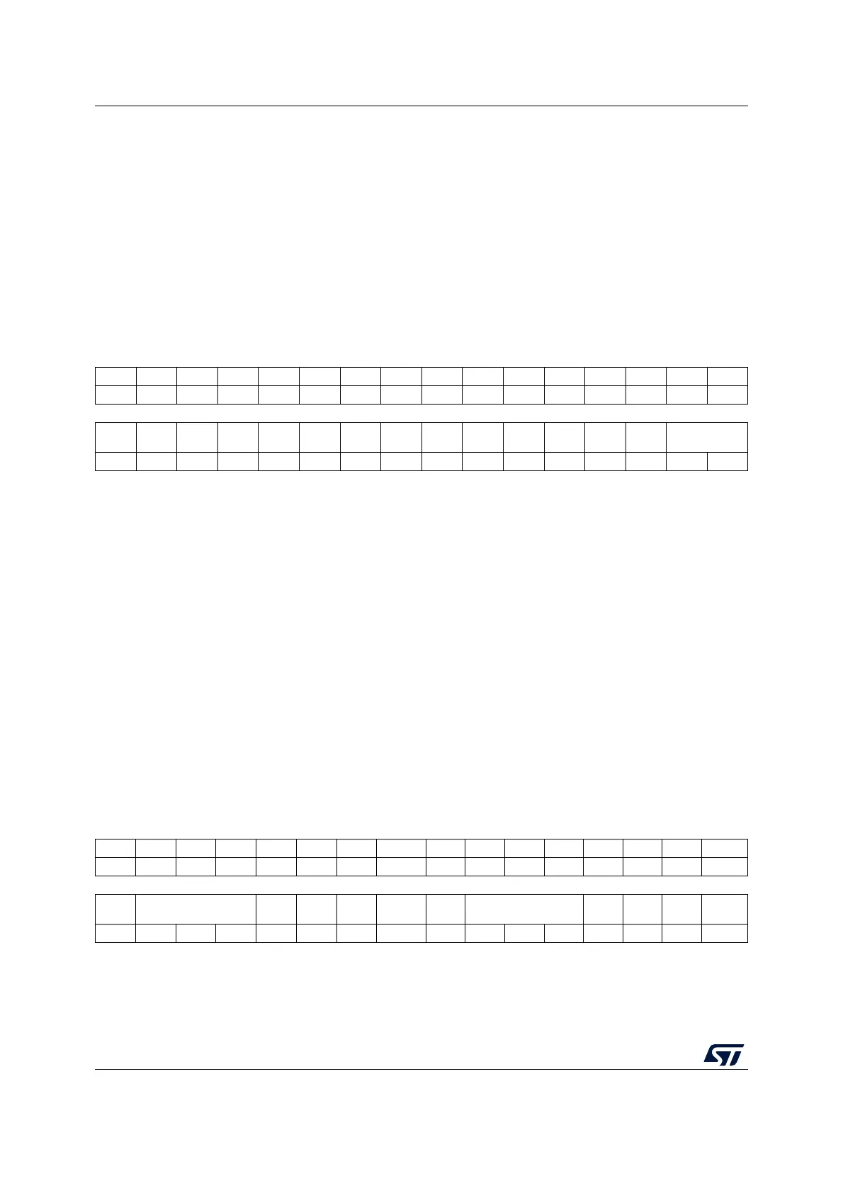
21.4.23 TIM1 option register 1 (TIM1_OR1)
Address offset: 0x50
Reset value: 0x0000 0000
21.4.24 TIM1 capture/compare mode register 3
(TIM1_CCMR3)
Address offset: 0x54
Reset value: 0x0000 0000
The channels 5 and 6 can only be configured in output.
Output compare mode:
Bits 31:0 DMAB[31:0]: DMA register for burst accesses
A read or write operation to the DMAR register accesses the register located at the address
(TIMx_CR1 address) + (DBA + DMA index) x 4
where TIMx_CR1 address is the address of the control register 1, DBA is the DMA base
address configured in TIMx_DCR register, DMA index is automatically controlled by the DMA
transfer, and ranges from 0 to DBL (DBL configured in TIMx_DCR).
31 30 29 28 27 26 25 24 23 22 21 20 19 18 17 16
Res. Res. Res. Res. Res. Res. Res. Res. Res. Res. Res. Res. Res. Res. Res. Res.
1514131211109876543210
Res. Res. Res. Res. Res. Res. Res. Res. Res. Res. Res. Res. Res. Res.
OCREF_CLR
[1:0]
rw rw
Bits 31:2 Reserved, must be kept at reset value.
Bit 1:0 OCREF_CLR[1:0]: Ocref_clr source selection
This bit selects the ocref_clr input source.
00: COMP1 output is connected to the OCREF_CLR input
01: COMP2 output is connected to the OCREF_CLR input
10: COMP3 output is connected to the OCREF_CLR input
11: Reserved
Note: COMP3 is available on STM32G0B1xx and STM32G0C1xx salestypes only.
31 30 29 28 27 26 25 24 23 22 21 20 19 18 17 16
Res. Res. Res. Res. Res. Res. Res. OC6M[3] Res. Res. Res. Res. Res. Res. Res. OC5M[3]
rw rw
1514131211109 8 7654321 0
OC6
CE
OC6M[2:0]
OC6
PE
OC6FE Res. Res.
OC5
CE
OC5M[2:0] OC5PE OC5FE Res. Res.
rw rw rw rw rw rw rw rw rw rw rw rw

 Loading...


