RM0444 Rev 5 89/1390
RM0444 Embedded Flash memory (FLASH)
118
Security option bytes
Flash memory address: 0x1FFF 7870
Reset value: 0x0000 0000 (ST production value)
3.4.2 FLASH option byte programming
After reset, the options related bits of the FLASH control register (FLASH_CR) are write-
protected. To run any operation on the option bytes page, the option lock bit OPTLOCK of
the FLASH control register (FLASH_CR) must be cleared. The following sequence is used
to unlock this register:
1. Unlock the FLASH_CR with the LOCK clearing sequence (refer to Unlocking the Flash
memory)
2. Write OPTKEY1=0x08192A3B of the FLASH option key register (FLASH_OPTKEYR)
3. Write OPTKEY2=0x4C5D6E7F of the FLASH option key register (FLASH_OPTKEYR)
Bits 31:9 Reserved, must be kept at reset value.
Bits 8:0 PCROP2B_END[8:0]: PCROP2B area end offset, Bank 2
PCROP2B_END contains the offset of the last PCROP subpage of the PCROP2B area in
Bank 2 of dual-bank devices.
Note: Values corresponding to addresses outside the Main memory are not allowed.
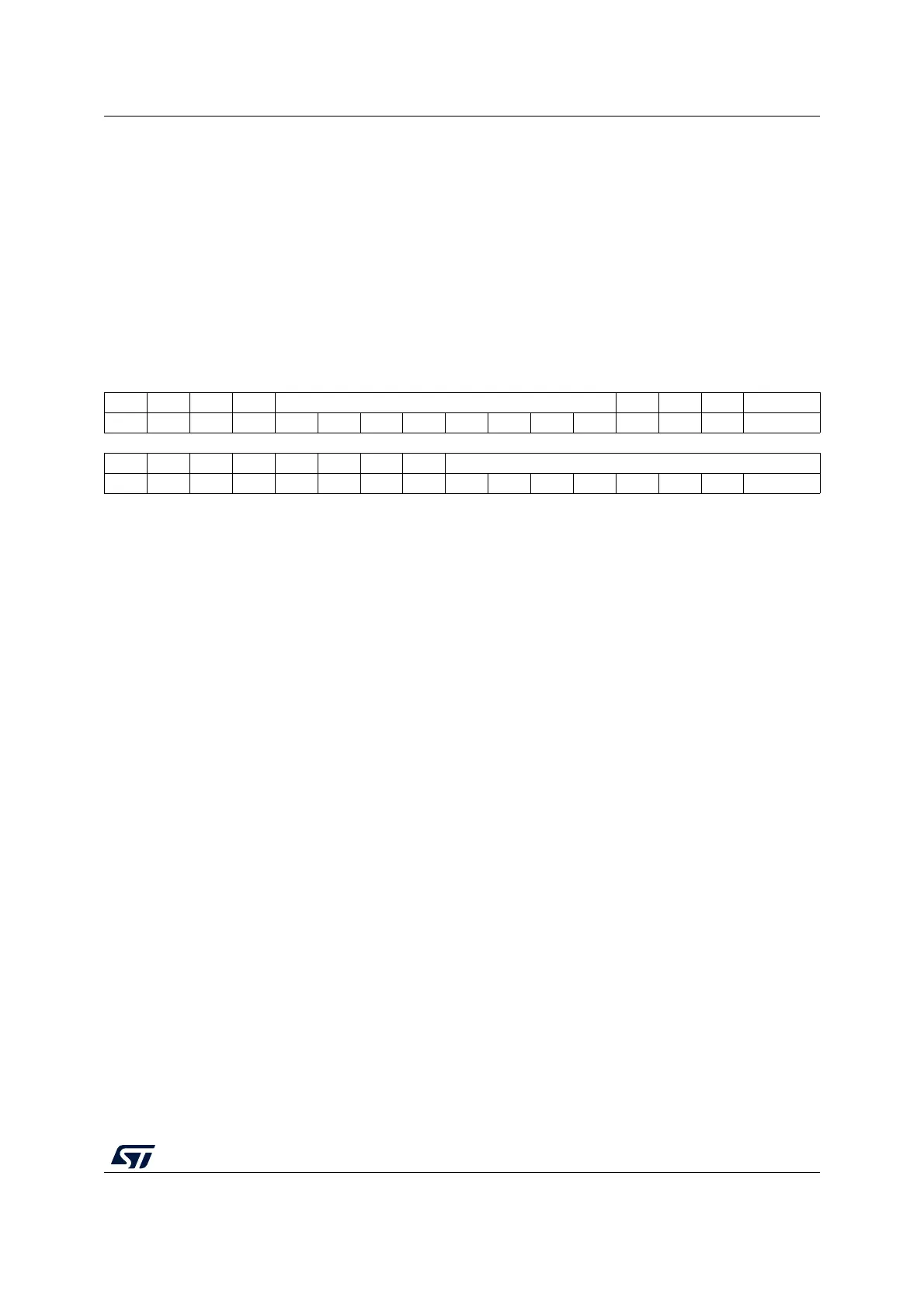
31 30 29 28 27 26 25 24 23 22 21 20 19 18 17 16
Res. Res. Res. Res. SEC_SIZE2[7:0] Res. Res. Res. BOOT_LOCK
rrrrrrrr r
151413121110987654321 0
Res. Res. Res. Res. Res. Res. Res. Res. SEC_SIZE[7:0]
rrrrrrr r
Bits 31:28 Reserved, must be kept at reset value.
Bits 27:20 SEC_SIZE2[7:0]: Securable memory area size, Bank 2
Contains the number of securable Flash memory pages in Bank 2 of dual-bank devices. In
single-bank devices, the bitfield is reserved.
Note: Values corresponding to addresses outside the Main memory are not allowed.
Bit 16 BOOT_LOCK: used to force boot from user area
0: Boot based on the pad/option bit configuration
1: Boot forced from Main Flash memory
Caution: If BOOT_LOCK is set in association with RDP Level 1, the debug capabilities of the
device are stopped and the reset value of the DBG_SWEN bit of the FLASH_ACR
register becomes zero. If DBG_SWEN bit is not set by the application code after
reset, there is no way to recover from this situation.
Bits 15:8 Reserved, must be kept at reset value.
Bits 7:0 SEC_SIZE[7:0]: Securable memory area size (Bank 1)
Contains the number of securable Flash memory pages (in Bank 1 for dual-bank devices).
Note: Values corresponding to addresses outside the Main memory are not allowed.

 Loading...


