General-purpose timers (TIM14) RM0444
730/1390 RM0444 Rev 5
24.4 TIM14 registers
The peripheral registers have to be written by half-words (16 bits) or words (32 bits). Read
accesses can be done by bytes (8 bits), half-words (16 bits) or words (32 bits).
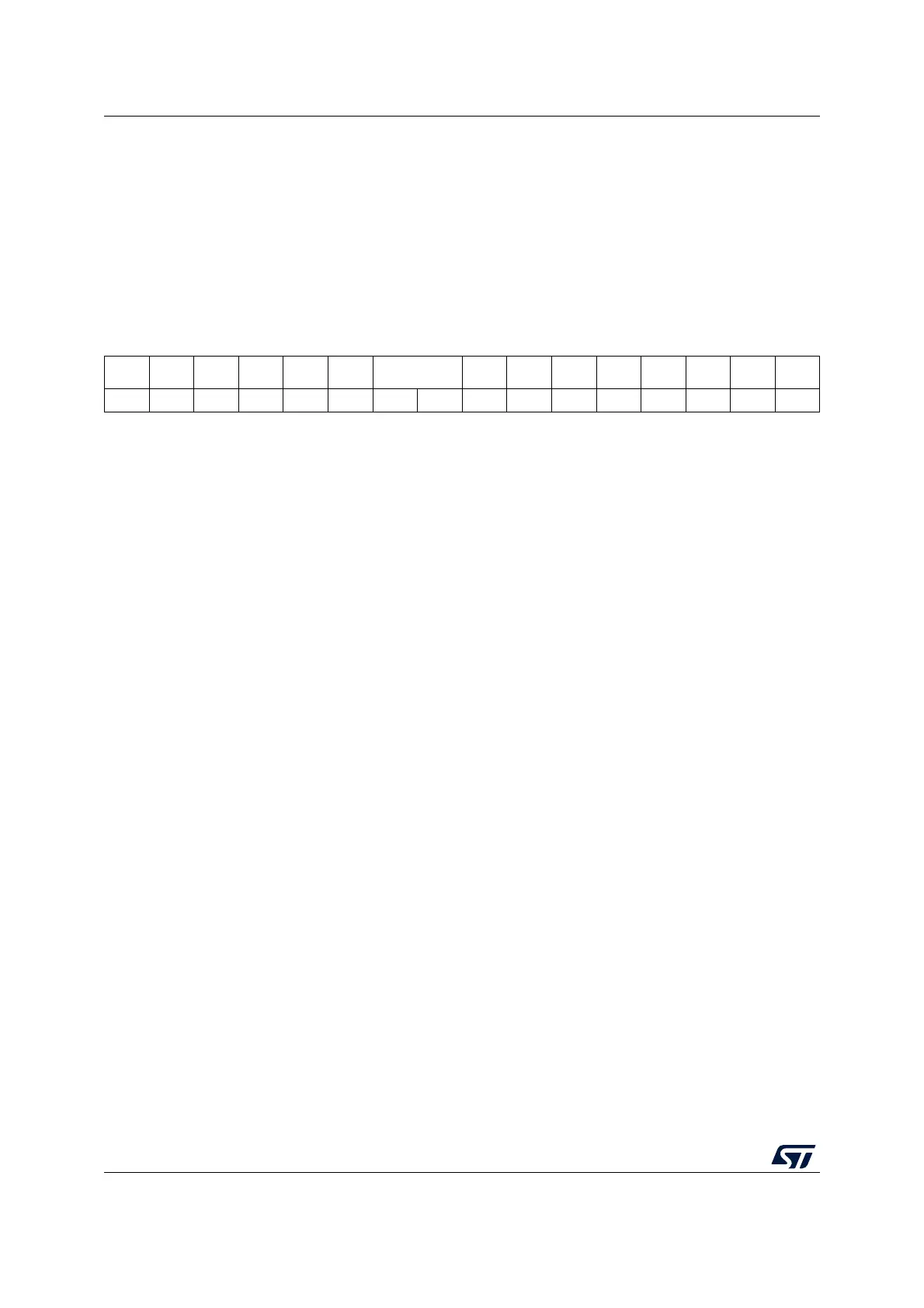
24.4.1 TIM14 control register 1 (TIM14_CR1)
Address offset: 0x00
Reset value: 0x0000
1514131211109876543210
Res. Res. Res. Res.
UIFRE
MAP
Res. CKD[1:0] ARPE Res. Res. Res. OPM URS UDIS CEN
rw rw rw rw rw rw rw rw
Bits 15:12 Reserved, must be kept at reset value.
Bit 11 UIFREMAP: UIF status bit remapping
0: No remapping. UIF status bit is not copied to TIMx_CNT register bit 31.
1: Remapping enabled. UIF status bit is copied to TIMx_CNT register bit 31.
Bit 10 Reserved, must be kept at reset value.
Bits 9:8 CKD[1:0]: Clock division
This bit-field indicates the division ratio between the timer clock (CK_INT) frequency and
sampling clock used by the digital filters (TIx),
00: t
DTS
= t
CK_INT
01: t
DTS
= 2 × t
CK_INT
10: t
DTS
= 4 × t
CK_INT
11: Reserved
Bit 7 ARPE: Auto-reload preload enable
0: TIMx_ARR register is not buffered
1: TIMx_ARR register is buffered
Bits 6:4 Reserved, must be kept at reset value.
Bit 3 OPM: One-pulse mode
0: Counter is not stopped on the update event
1: Counter stops counting on the next update event (clearing the CEN bit).

 Loading...


