RM0444 Rev 5 507/1390
RM0444 AES hardware accelerator (AES)
522
20.4.14 AES key registers
The AES_KEYRx write-only registers store the encryption or decryption key bitfield
KEY[127:0] or KEY[255:0]. The data to write to each register is organized in the memory in
little-endian order, that is, with most significant byte on the highest address (reads are not
allowed for security reason).
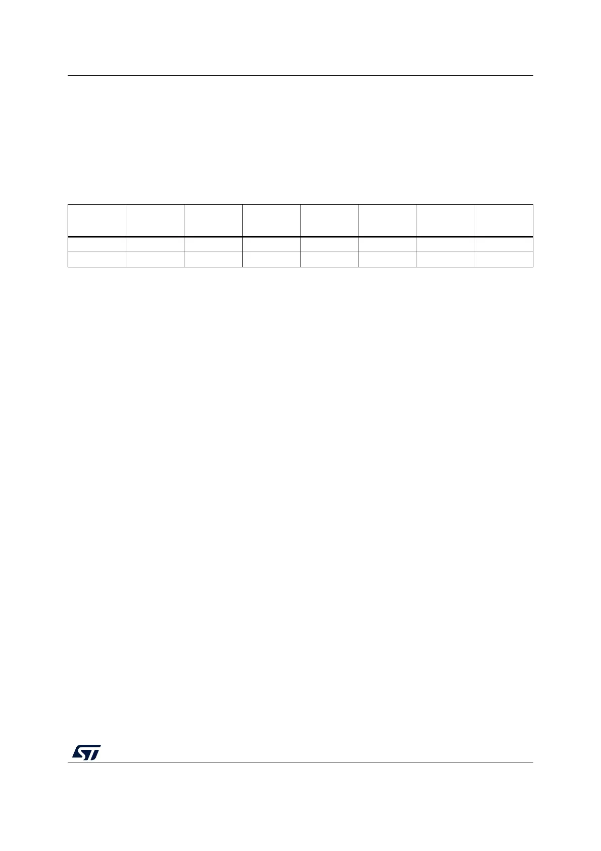
The key is spread over eight registers as shown in Table 107.
The key for encryption or decryption may be written into these registers when the AES
peripheral is disabled, by clearing the EN bit of the AES_CR register.
The key registers are not affected by the data swapping controlled by DATATYPE[1:0]
bitfield of the AES_CR register.
20.4.15 AES initialization vector registers
The four AES_IVRx registers keep the initialization vector input bitfield IVI[127:0]. The data
to write to or to read from each register is organized in the memory in little-endian order, that
is, with most significant byte on the highest address. The registers are also ordered from
lowest address (AES_IVR0) to highest address (AES_IVR3).
The signification of data in the bitfield depends on the chaining mode selected. When used,
the bitfield is updated upon each computation cycle of the AES core.
Write operations to the AES_IVRx registers when the AES peripheral is enabled have no
effect to the register contents. For modifying the contents of the AES_IVRx registers, the EN
bit of the AES_CR register must first be cleared.
Reading the AES_IVRx registers returns the latest counter value (useful for managing
suspend mode).
The AES_IVRx registers are not affected by the data swapping feature controlled by the
DATATYPE[1:0] bitfield of the AES_CR register.
20.4.16 AES DMA interface
The AES peripheral provides an interface to connect to the DMA (direct memory access)
controller. The DMA operation is controlled through the AES_CR register.
Data input using DMA
Setting the DMAINEN bit of the AES_CR register enables DMA writing into AES. The AES
peripheral then initiates a DMA request during the input phase each time it requires to write
a 128-bit block (quadruple word) to the AES_DINR register, as shown in Figure 99.
Note: According to the algorithm and the mode selected, special padding / ciphertext stealing
might be required. For example, in case of AES GCM encryption or AES CCM decryption, a
Table 107. Key endianness in AES_KEYRx registers (128- or 256-bit key length)
AES_KEYR7
[31:0]
AES_KEYR6
[31:0]
AES_KEYR5
[31:0]
AES_KEYR4
[31:0]
AES_KEYR3
[31:0]
AES_KEYR2
[31:0]
AES_KEYR1
[31:0]
AES_KEYR0
[31:0]
- - - - KEY[127:96] KEY[95:64] KEY[63:32] KEY[31:0]
KEY[255:224] KEY[223:192] KEY[191:160] KEY[159:128] KEY[127:96] KEY[95:64] KEY[63:32] KEY[31:0]

 Loading...


